Thin film photovoltaic module having a lamination layer for enhanced reflection and photovoltaic output

a technology of photovoltaic modules and lamination layers, applied in photovoltaics, electrical devices, semiconductor devices, etc., can solve the problems and inability to meet the needs etc., to reduce the process steps of photovoltaic active layer stacks, reduce the effect of complex and expensive process steps

Inactive Publication Date: 2011-01-27
SURYA POWER
View PDF10 Cites 14 Cited by
  • Summary
  • Abstract
  • Description
  • Claims
  • Application Information

AI Technical Summary

Benefits of technology

[0013](a) reduced photovoltaic active layer stack process steps, and thus the potential to standardize equipment for the deposition or growth of the light absorbing thin films;
[0014](b) simplified prevention of moisture ingress, thereby eliminating complex, expensive process steps, and reducing the capital cost of processing equipment;
[0015](c) higher thin film PV module efficiency.

Problems solved by technology

Linking conventional solar cells together into a PV module results in gaps between cells.
Compared to conventional crystalline silicon solar cells, thin-film solar cells exhibit less efficiency for converting sunlight to usable electric power.
In such a conventional thin film PV module, providing reflectance to the back of the thin film stack is complex and expensive, since it requires extra deposition process steps, adds process time, and requires significant capital expenditure for processing equipment.
A disadvantage in the construction of a conventional thin film PV module is that the lamination materials are not filled and are not thermally conductive.
Conventional thin film lamination materials tend to be thermally insulative, and thereby cause undesirable retention of heat upon prolonged exposure to the sun.
Since there is no way for heat to escape, conventional thin film PV cells exhibit reduced efficiency as their temperature increases.

Method used


Image

  • Thin film photovoltaic module having a lamination layer for enhanced reflection and photovoltaic output
  • Thin film photovoltaic module having a lamination layer for enhanced reflection and photovoltaic output
  • Thin film photovoltaic module having a lamination layer for enhanced reflection and photovoltaic output

Examples


Embodiment Construction

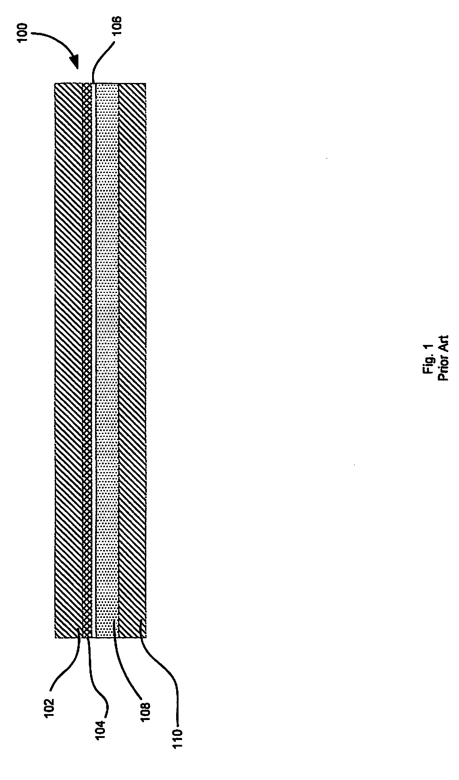
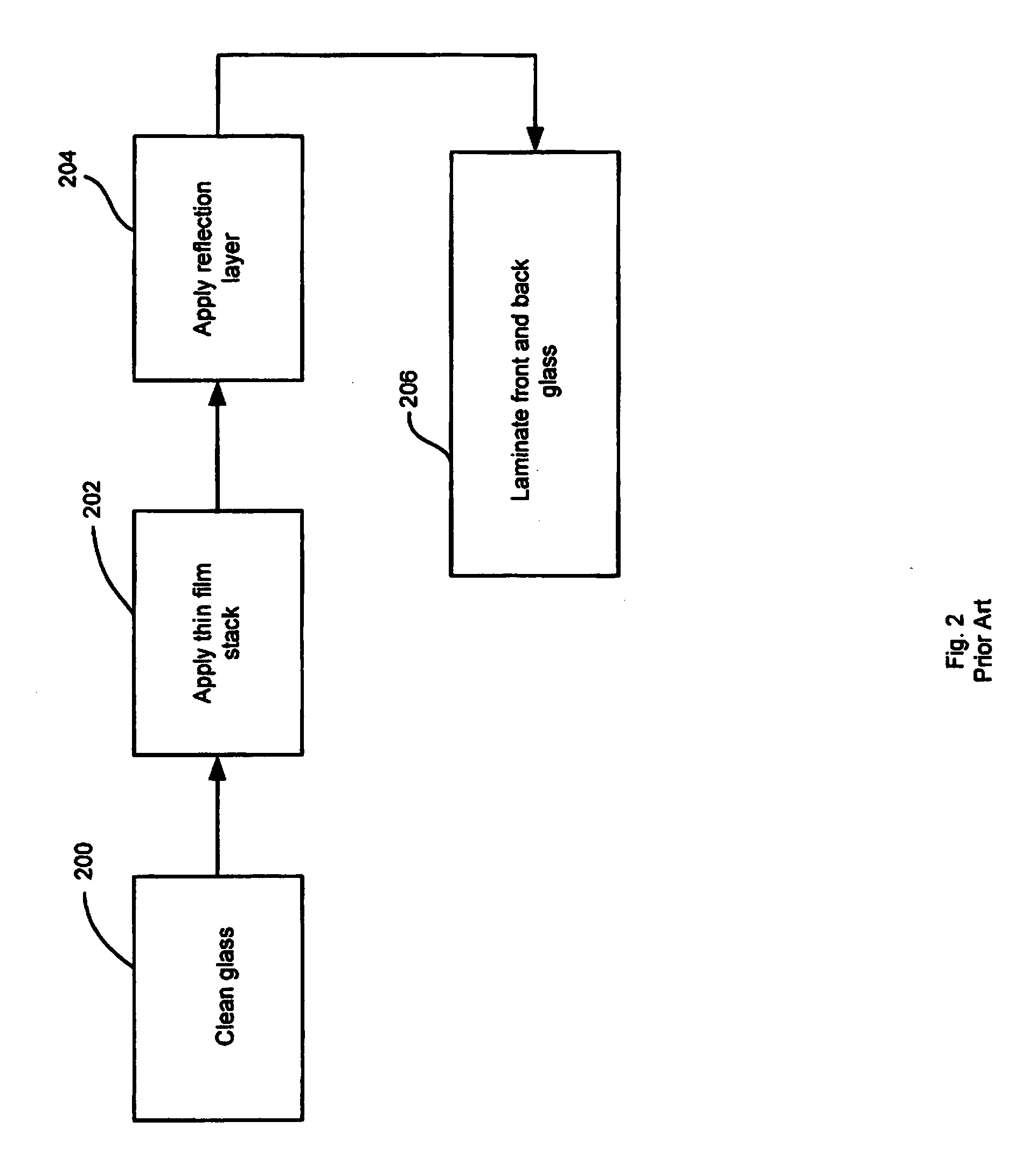
[0024]Referring to the drawings, FIGS. 1 and 2 show a cross section of a conventional thin film PV module 100 and a standard process for making the PV module, respectively. The thin film PV module comprises a transparent substrate 102 such as glass. A light absorbing thin film stack 104 is provided on the interior side of transparent substrate 102 using multiple semiconductor processing steps. An example of a conventional process for forming a light absorbing thin film stack is shown in Schicht et al., U.S. Pat. No. 6,159,621 incorporated herein by reference. The thin film stack 104 can be formed by any well known thin-film PV technology including epitaxial Si, copper indium gallium deselenide (CIGS), cadmium telluride (CdTe), or the like.

[0025]Referring to FIG. 1 and the process in FIG. 2, transparent substrate 102 typically comprises a transparent substrate such as glass that is carefully cleaned as shown at 202 prior to the application of the light-absorbing thin film stack 104. ...


PUM


Abstract

An improved thin film PV module and simplified fabrication process are provided that achieve higher PV module efficiency, while eliminating expensive process steps, and reducing the capital cost of thin film processing equipment. A lamination material, characterized by high reflectivity as well as thermal conductivity and emissivity, is provided directly adjacent the active region of a thin film stack, eliminating the need for complex sputtering or deposition process steps ordinarily required for providing a reflective layer. The lamination material reflects unabsorbed light back into the thin film stack, thereby increasing photocurrent generation, and obviating the need for a reflective metallization layer. The lamination layer and back sheet for sealing the light-absorbing stack against the ingress of moisture also can be applied in a single process step.

Description

CROSS REFERENCE TO RELATED APPLICATION[0001]This application claims the benefit of U.S. provisional patent application Ser. No. 61 / 271,775, filed Jul. 24, 2009.BACKGROUND[0002]1. Field of the Invention[0003]The field of the invention generally relates to photovoltaic (PV) modules. In particular, the field of the invention relates to an easily manufactured thin film PV module comprising a lamination sheet characterized by high reflectance for reflecting the unabsorbed solar radiation back into the thin film stack, resulting in enhanced photo current generation, and for simplifying the semiconductor process steps for the thin film stack.[0004]2. Background of Related Art[0005]As is well known, in a thin film photovoltaic solar cell, solar radiation is absorbed by the active thin film layer of semiconductor material resulting in generation of electrons and holes. The electrons and holes are separated by a built-in electric field, such as a rectifying junction, as in a conventional sola...

Claims


Application Information

Patent Timeline
Patent Type & Authority Applications(United States)
IPC IPC(8): H01L31/18H01L31/00
CPCH01L31/02327Y02E10/52H01L31/052H01L31/048H02S40/22H02S40/42H01L31/0445
Inventor FARRELL, JAMES F.PEDDADA, SATYANARAYANA RAO
Owner SURYA POWER
Why Eureka
Try Eureka