Sodium doping method and system of cigs based materials using large scale batch processing

a technology of cigs and materials, applied in the field of photovoltaic materials and manufacturing methods, can solve the problems of reducing the reducing the production efficiency reducing the production cost of cigs based materials, etc., and achieves the effect of reducing the production cos

Inactive Publication Date: 2011-01-27
CM MFG
View PDF21 Cites 10 Cited by
  • Summary
  • Abstract
  • Description
  • Claims
  • Application Information

AI Technical Summary

Benefits of technology

[0011]Many benefits can be achieved by applying the embodiments of the present invention. Particularly, a sodium doping process serves an important step for forming copper based chalcopyrite structured high efficiency photovoltaic absorber layer. The present invention provides a efficient way using large scale batch system processing to perform the sodium doping to achieve a well controlled sodium concentration in the formed absorber layer. The method simplifies the doping process through a specific configuration of a plurality of soda lime glass substrates that come from the same batch system. The sodium doping process also can be advantageously performed in a same thermal treatment process of forming a photovoltaic absorber layer of copper indium diselenide (CIS) or copper indium gallium diselenide (CIGS) in chalcopyrite structure with large grain sizes for achieving high efficiency of thin film solar cells thereof. Of course, there can be other variations, modifications, and alternatives.

Problems solved by technology

Unfortunately, the supply of petrochemical fuel is limited and essentially fixed based upon the amount available on the planet Earth.
Additionally, as more people use petroleum products in growing amounts, it is rapidly becoming a scarce resource, which will eventually become depleted over time.
Although solar energy is environmentally clean and has been successful to a point, many limitations remain to be resolved before it becomes widely used throughout the world.
However, crystalline materials are often costly and difficult to make on a large scale.
Additionally, devices made from such crystalline materials often have low energy conversion efficiencies.
Similar limitations exist with the use of thin film technology in making solar cells.
That is, efficiencies are often poor.
Additionally, film reliability is often poor and cannot be used for extensive periods of time in conventional environmental applications.
Often, thin films are difficult to mechanically integrate with each other.
Furthermore, integration of electrode layers, substrates with uncontrolled sodium content, and overlying absorber layers is also problematic.

Method used


Image

  • Sodium doping method and system of cigs based materials using large scale batch processing
  • Sodium doping method and system of cigs based materials using large scale batch processing
  • Sodium doping method and system of cigs based materials using large scale batch processing

Examples


Embodiment Construction

[0015]The present invention relates generally to photovoltaic materials and manufacturing method. More particularly, the present invention provides a method and system for fabricating thin film solar cells. Merely by way of example, the present method includes a sodium doping method for manufacture of CIGS based photovoltaic cells using on a large scale batch processing, but it would be recognized that the invention may have other configurations.

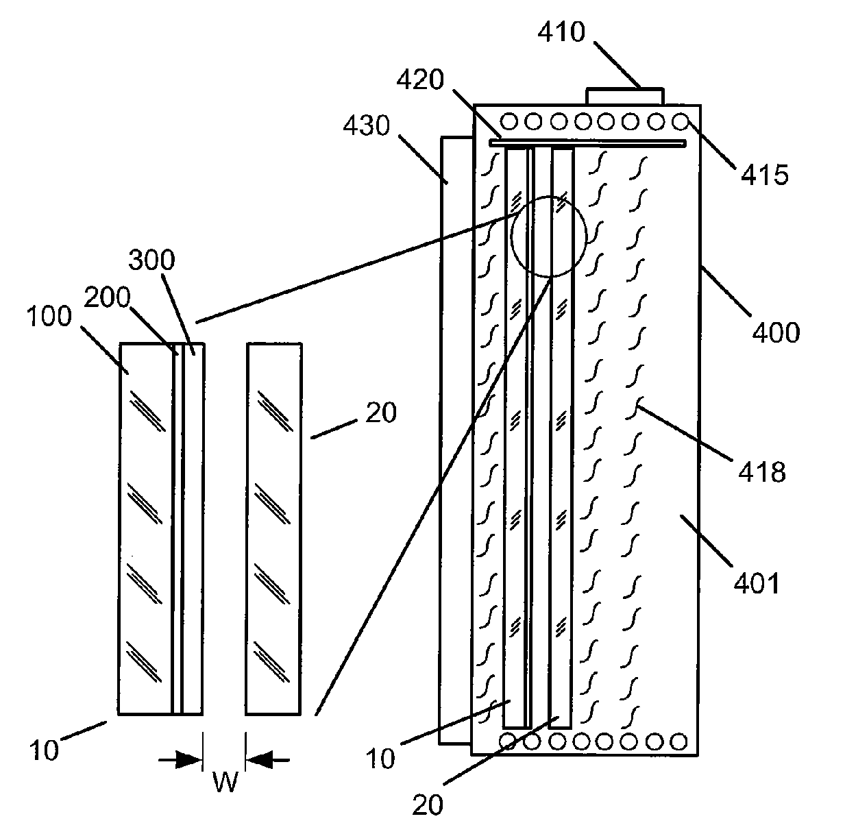
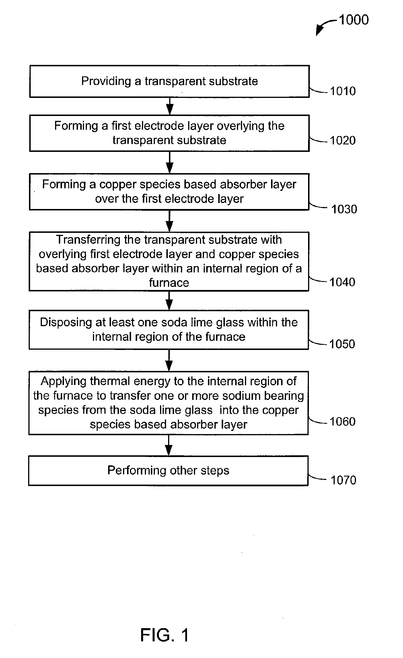
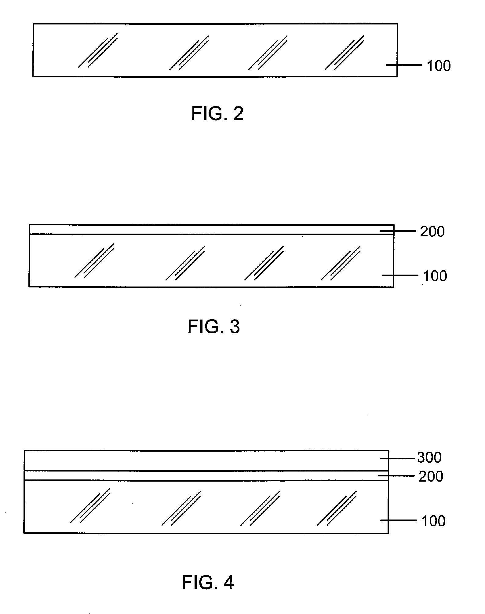
[0016]FIG. 1 is a simplified flowchart illustrating a method of fabricating a thin film photovoltaic cell according to an embodiment of the present invention. This diagram is merely an example, which should not unduly limit the scope of the claims herein. The method 1000 includes the following processes:[0017]1. Process 1010 for providing at least one transparent substrate;[0018]2. Process 1020 for forming a first electrode layer overlying the transparent substrate;[0019]3. Process 1030 for forming a copper species based absorber precursor l...


PUM

PropertyMeasurementUnit
grain sizesaaaaaaaaaa
pressureaaaaaaaaaa
thicknessaaaaaaaaaa

Abstract

A method of processing a plurality of photovoltaic materials in a batch process includes providing at least one transparent substrate having an overlying first electrode layer and an overlying copper species based absorber precursor layer within an internal region of a furnace. The overlying copper species based absorber precursor layer has an exposed face. The method further includes disposing at least one soda lime glass comprising a soda lime glass face within the internal region of the furnace such that the soda lime glass face is adjacent by a spacing to the exposed face of the at least one transparent substrate. Furthermore, the method includes subjecting the at least one transparent substrate and the one soda lime glass to thermal energy to transfer one or more sodium bearing species from the soda lime glass face across the spacing into the copper species based absorber precursor layer via the exposed face.

Description

CROSS-REFERENCES TO RELATED APPLICATIONS[0001]This application claims priority to U.S. Provisional Patent Application No. 61 / 101,662, filed Sep. 30, 2008, entitled “SODIUM DOPING METHOD AND SYSTEM OF CIGS BASED MATERIALS USING LARGE SCALE BATCH PROCESSING” by inventor Robert D. Wieting, commonly assigned and incorporated by reference herein for all purposes.STATEMENT AS TO RIGHTS TO INVENTIONS MADE UNDER FEDERALLY SPONSORED RESEARCH AND DEVELOPMENT[0002]Not ApplicableREFERENCE TO A “SEQUENCE LISTING,” A TABLE, OR A COMPUTER PROGRAM LISTING APPENDIX SUBMITTED ON A COMPACT DISK[0003]Not ApplicableBACKGROUND OF THE INVENTION[0004]The present invention relates generally to photovoltaic materials and manufacturing method. More particularly, the present invention provides a method and system for fabricating thin film solar cells. Merely by way of example, the present method includes a sodium doping method for manufacture of CIGS based photovoltaic cells using on a large scale batch proces...

Claims


Application Information

Patent Timeline
Patent Type & Authority Applications(United States)
IPC IPC(8): H01L21/30
CPCC03C17/002C03C2218/32Y02E10/541H01L31/0392H01L31/1876H01L31/0322H01L31/03923Y02P70/50
Inventor WIETING, ROBERT D.
Owner CM MFG
Why Eureka
Try Eureka