Circuit Substrate and Structure Using the Same

a technology of circuit substrate and structure, applied in the field of circuit substrate, can solve the problems of cracks growing along the gap between them in a vertical direction, cracks in the resin layer of ionized conductive materials, and more likely cracks in the resin layer, so as to reduce the possibility of short circuit, suppress the growth of cracks, and reduce the effect of short circui

Inactive Publication Date: 2011-02-03
KYOCERA CORP
View PDF5 Cites 10 Cited by
  • Summary
  • Abstract
  • Description
  • Claims
  • Application Information

AI Technical Summary

Benefits of technology

[0010]The circuit substrate can suppress a growth of crack generated in the base, thereby reducing a short circuit between the conductive

Problems solved by technology

In such cases, because of a difference in coefficient of thermal expansion between a resin material and the filler which are contained in the resin layers, the resin material and the filler may separate from each other, and a crack may grow along a gap separating them in a vertical direction.
On the other hand, during use of the circuit substrate, there is a possibility that when a voltage is applied between the conductive layers s

Method used


Image

  • Circuit Substrate and Structure Using the Same
  • Circuit Substrate and Structure Using the Same
  • Circuit Substrate and Structure Using the Same

Examples


Embodiment Construction

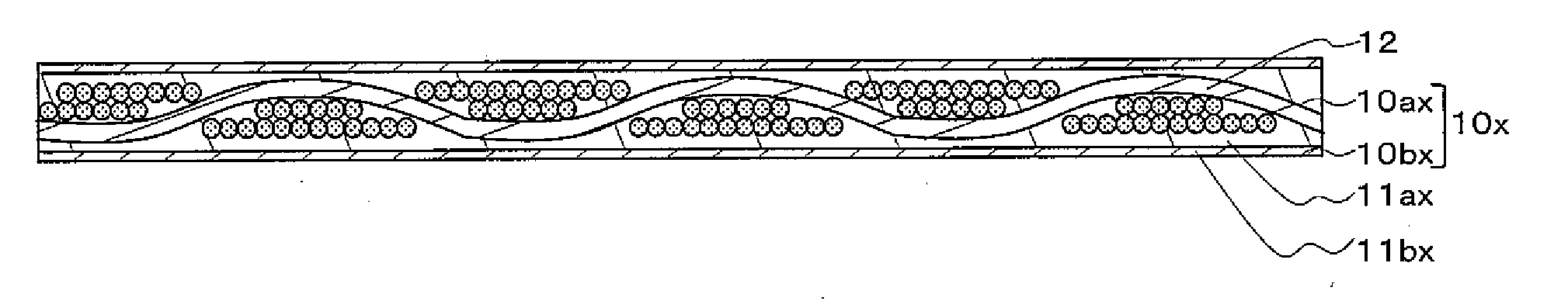
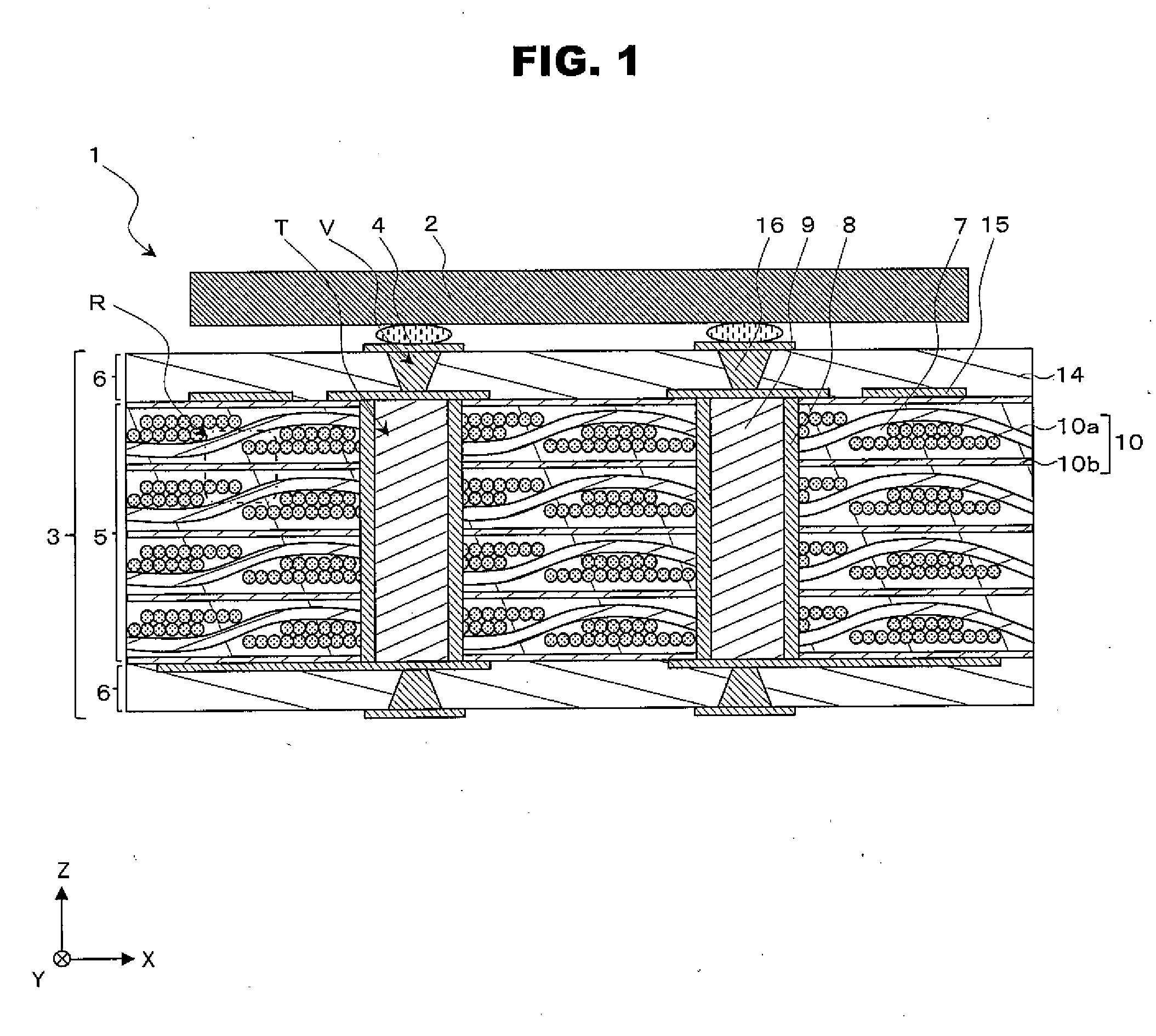
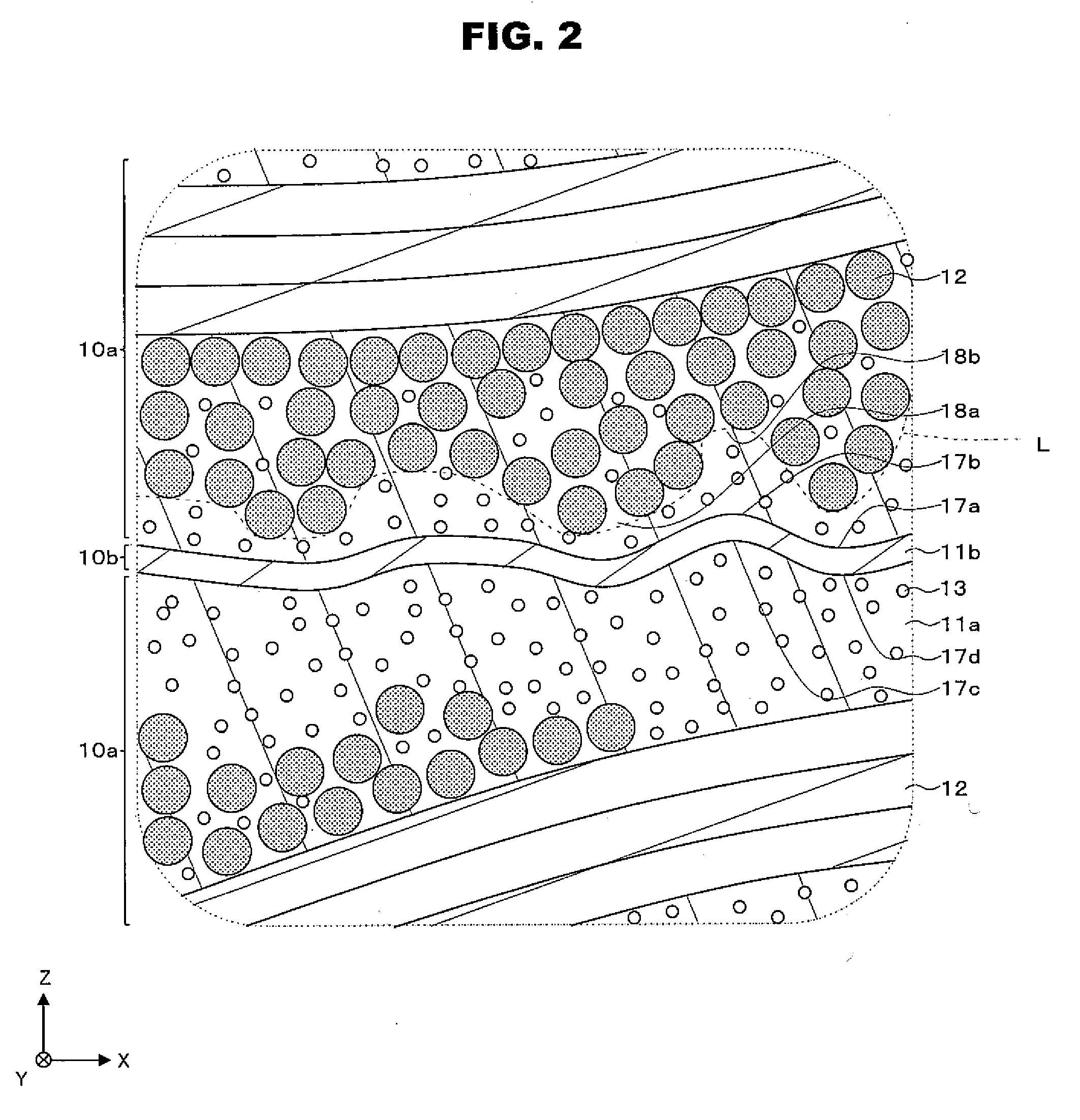
[0044]A circuit substrate and a mounting structure according to an embodiment of the present invention are described below in detail with reference to the attached drawings.

[0045]A mounting structure 1 shown in FIG. 1 is used for various electronic apparatuses such as audiovisual apparatuses, electrical appliances, communication apparatuses, computer apparatuses, and the peripheral devices thereof. The mounting structure 1 includes an electronic component 2 and a circuit substrate 3.

[0046]The electronic component 2 is a semiconductor device such as IC or LSI. The electronic component may be mounted on the circuit substrate 3 through a bump 4 such as solder using a flip chip packaging technology.

[0047]The parent material of this electronic component 2 is composed of a semiconductor material, for example, silicon, germanium, gallium arsenide, gallium-arsenic-phosphorus, gallium nitride, silicon carbide, or the like. As the electronic component 2, a component having a thickness of, for...


PUM

PropertyMeasurementUnit
Percent by volumeaaaaaaaaaa
Thicknessaaaaaaaaaa
Volumeaaaaaaaaaa

Abstract

A circuit substrate comprises a base and conductive layers disposed on lower and upper surfaces of the substrate. The base includes resin layers and the conductive layers overlapping with each other in a plan view. The resin layers include first resin layers and a second resin layer interposed between the first resin layers. The first resin layer has a filler and the second resin layer has no filler or a filler whose amount is 1 volume % or less and smaller than an amount of the filler in the first resin layer.

Description

CROSS REFERENCE TO RELATED APPLICATION(S)[0001]The present application claims priority under 35 U.S.C. §119 to Japanese Patent Application No. 2009-175286, filed on Jul. 28, 2009, entitled “CIRCUIT SUBSTRATE”, the entirety of which is incorporated by reference herein.BACKGROUND OF THE INVENTION[0002]1. Field of the Invention[0003]The present invention relates to a circuit substrate used for electronic apparatuses (e.g., audiovisual apparatuses, electrical appliances, communication apparatuses, computer apparatuses, and the peripheral devices thereof).[0004]2. Description of the Related Art[0005]Hitherto, a mounting structure in which mounting electronic components are mounted on a circuit substrate has been used.[0006]Japanese Unexamined Patent Application Publication No. 2008-120922 describes a circuit substrate including a base that includes a plurality of resin layers stacked one above another, and conductive layers formed on upper and lower surfaces of the base.[0007]To increase...

Claims


Application Information

Patent Timeline
IPC IPC(8): H05K1/00
CPCH05K1/036H05K1/0366H05K2201/029H05K3/4602H05K2201/0209H05K1/0373H01L2224/16225
Inventor NAGASAWA, TADASHI
Owner KYOCERA CORP
Why Eureka
Try Eureka