Substrate bias for CMOS imagers

a cmos imager and substrate bias technology, applied in the field of imaging devices, can solve the problems of high manufacturing cost of ccds, ccd imagers suffer from a number, and ccds are susceptible to radiation damag

Active Publication Date: 2011-02-03
SRI INTERNATIONAL
View PDF15 Cites 45 Cited by
  • Summary
  • Abstract
  • Description
  • Claims
  • Application Information

AI Technical Summary

Benefits of technology

[0023]According to an embodiment of the present invention, the at least one CMOS pixel further comprises a first charge transfer gate located between the sense node and the phototransistor. A second charge transfer gate located adjacent the phototransistor and distal to the first transfer gate and a highly doped contact of the first conductivity type is formed in the semiconductor substrate and configured for receiving a potential for providing a global reset of the at least one pixel and for preventing charge carriers from blooming to the sense node.

Problems solved by technology

However, CCD imagers suffer from a number of disadvantages.
For example, CCDs are susceptible to radiation damage; CCDs are often expensive to manufacture; CCDs require good light shielding to avoid image smear and; CCDs have a high power dissipation for large arrays.
CCD imagers also have a complicated driving method and a complicated fabrication process requiring a multi-phased photo process.
A control circuit, a signal processing circuit, an analog to digital (A / D) converter circuit, etc., cannot be easily integrated into a CCD chip, thereby inhibiting the use of CCDs in compact size products.
While there have been some attempts to integrate on-chip signal processing with a CCD array, these attempts have not been entirely successful.
CCDs may also suffer from incomplete charge transfer from pixel to pixel during charge transfer which also results in image smear.
When a CCD imager is illuminated on the front side, absorption of incident light by the electronic circuitry reduces quantum efficiency.
As an alternative, CCDs may be illuminated from the back side; however, back side illumination produces other problems.
Therefore, for good blue and ultraviolet response, the substrate must be extremely thin in order to have acceptable charge spreading (crosstalk), resulting in a very fragile and expensive structure.
Compared to CCDs, low pixel cross talk is more difficult to achieve for the CMOS imagers described in the '085 patent, especially for thick imagers that detect near IR and x-ray photons.
However, even when silicon is fully depleted, the desired low cross talk may not be realized.
However, the technique is considerably more difficult to implement in CMOS compared to CCDs.

Method used


Image

  • Substrate bias for CMOS imagers
  • Substrate bias for CMOS imagers
  • Substrate bias for CMOS imagers

Examples


Embodiment Construction

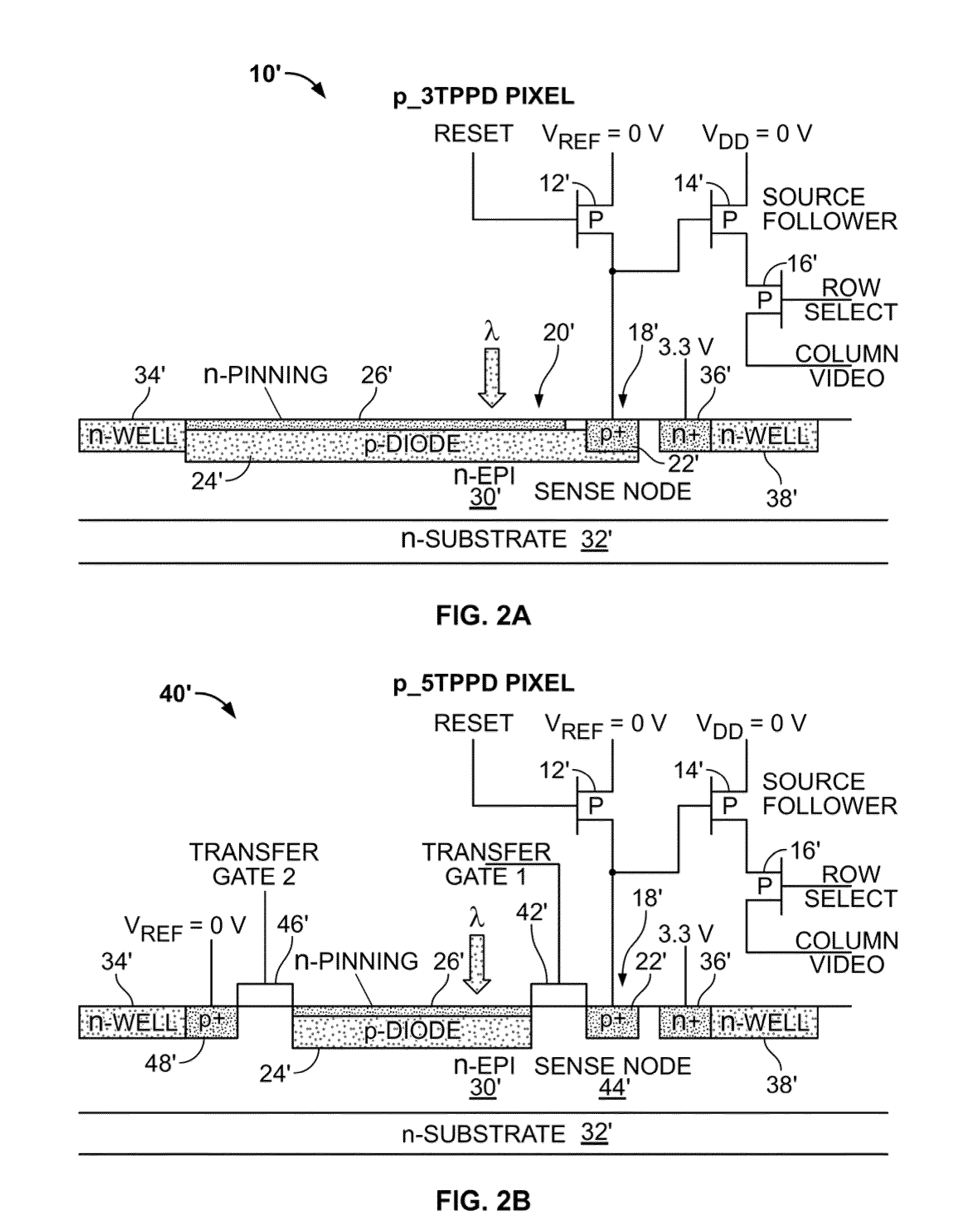
[0057]FIGS. 2A and 2B are cross-sectional views of CMOS pixels having substantially corresponding structures to the pixels of FIGS. 1A and 1B with doping conductivity types reversed, according to an embodiment of the present invention. The CMOS pixels are hereinafter designated as p—3TPPD and p—5TPPD pixels, 10′, 40′, respectively. The p—3TPPD pixel 10′ includes three PMOS transistors 12′, 14′, 16′ standing for a reset transistor 12′, a source follower transistor 14′ and a row transistor 16′. The reset transistor 12′ is electrically connected to a sense node 18′. The sense node 18′ is formed of a p+ contact 22′ and a pinned photodiode 20′. The pinned photodiode 20′ includes a thin n-type pinning layer 26′ overlying a custom p-diode implant 24′, that in turn, overlies and forms a depletion region with an n-epitaxial layer 30′. An n-substrate 32′ underlies the n-epitaxial layer 30′. An n-well 34′ is formed adjacent the pinned photodiode 20′ in the n-epitaxial layer 30′ for isolating t...


PUM


Abstract

A CMOS image sensor is disclosed. The CMOS imager includes a lightly doped semiconductor substrate of a first conductivity type. At least one CMOS pixel of a second conductivity type is formed in the semiconductor substrate. The semiconductor substrate is configured to receive a bias voltage applied for substantially depleting the semiconductor substrate and for forming a depletion edge within the semiconductor substrate. A well of the second conductivity type substantially surrounds the at least one CMOS pixel to form a depletion region about the at least one CMOS pixel operable to form a minimum predetermined barrier to the depletion edge within the semiconductor substrate to pinch off substrate bias in proximity to the return contact.

Description

CROSS-REFERENCE TO RELATED APPLICATIONS[0001]This application claims the benefit of U.S. provisional patent application No. 61 / 230,440 filed Jul. 31, 2009 and U.S. provisional patent application No. 61 / 358,921 filed Jun. 27, 2010, the disclosures of which are incorporated herein by reference their entirety.FIELD OF THE INVENTION[0002]The invention relates generally to imaging devices. More specifically, the invention relates to improving the performance of CMOS imagers by exploiting substrate bias techniques.BACKGROUND OF THE INVENTION[0003]Generally, an image sensor is a semiconductor device for converting an optical image into an electric signal. There are a number of different types of semiconductor-based imagers, including charge coupled devices (CCDs), photodiode arrays, charge injection devices, hybrid focal plane arrays, etc. The various types of image sensors may be broadly categorized as charge coupled devices (CCD) and complementary metal oxide semiconductor (CMOS) image s...

Claims


Application Information

Patent Timeline
Patent Type & Authority Applications(United States)
IPC IPC(8): H01L31/112H01L31/18
CPCH01L27/14609H01L27/14658H01L27/14643H01L31/109H01L27/14689
Inventor JANESICK, JAMES ROBERT
Owner SRI INTERNATIONAL
Why Eureka
Try Eureka