Semiconductor device and method for manufacturing the same

a semiconductor chip and semiconductor technology, applied in the direction of semiconductor/solid-state device testing/measurement, mechanical measuring arrangement, instruments, etc., can solve the problems of reduced semiconductor chip size, circuit design becomes complicated, packaging defect, etc., and achieve the effect of complicated circuit design

Active Publication Date: 2011-02-03
RENESAS ELECTRONICS CORP
View PDF6 Cites 24 Cited by
  • Summary
  • Abstract
  • Description
  • Claims
  • Application Information

AI Technical Summary

Benefits of technology

[0023]The following is a brief description of an effect obtained by the typical invention out of the inventions disclosed herein.
[0024]An electrical characteristics test for a semiconductor i...

Problems solved by technology

There also has been pointed out the problem that if a probe is brought into contact with an external coupling terminal (solder ball) in a package during the electrical characteristic test in the post-process, there remains a probe trace on the solder ball and the probe trace causes a packaging defect.
However, if an attempt is made to measure a circuit impedance with use of the foregoing Kelvin contact method (or four-terminal mea...

Method used


Image

  • Semiconductor device and method for manufacturing the same
  • Semiconductor device and method for manufacturing the same
  • Semiconductor device and method for manufacturing the same

Examples


first embodiment

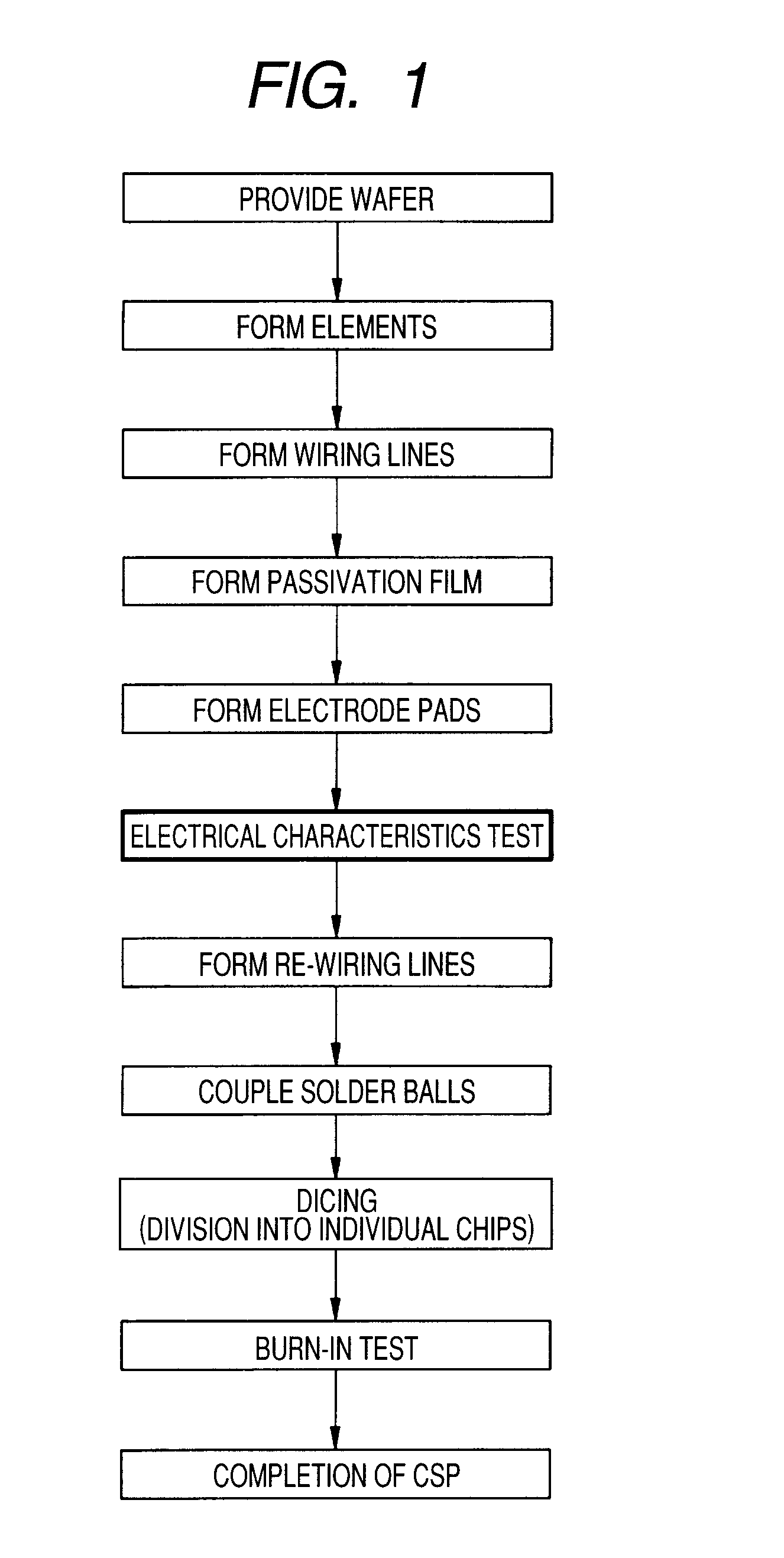
[0050]This embodiment is an application of the present invention to the manufacture of a CSP which is a kind of a surface mount type semiconductor package. FIG. 1 is an entire flow chart showing a manufacturing process for the CSP.

[0051]One feature of this manufacturing process resides in that, in order to greatly shorten the post-process and implement a CSP (RCSP: Real Chip Size Package) of substantially the same size as a semiconductor chip, re-wiring lines are provided using Al (aluminum) or Cu (copper) over existing wiring lines on a semiconductor wafer (hereinafter referred to simply as “wafer”) with semiconductor chips arranged in plural rows and plural columns, and a plurality of external coupling terminals (solder balls) are coupled electrically onto the re-wiring lines and are arranged on the wafer.

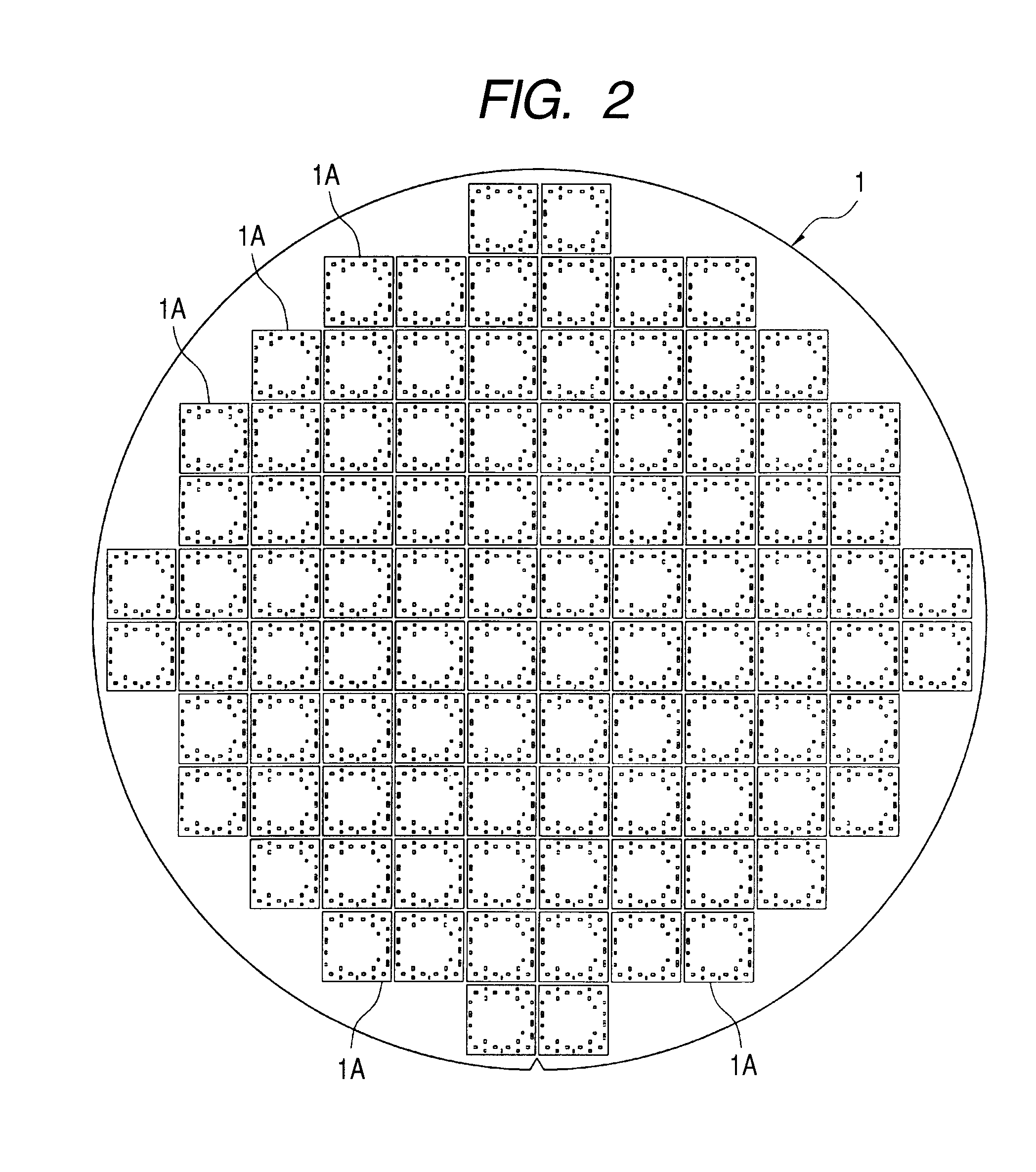
[0052]For fabricating the CSP formed in the above manner, first a semiconductor wafer formed by single crystal silicon is provided and elements such as MOSFETs are formed on a ma...

second embodiment

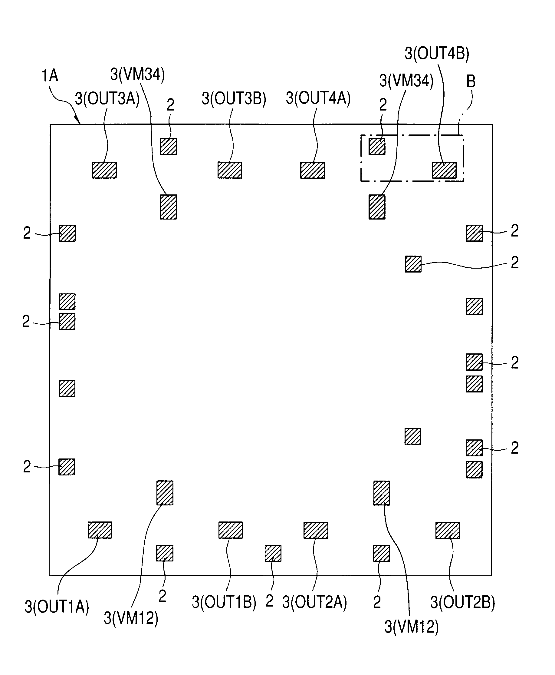
[0076]In the above first embodiment a description has been given about performing Kelvin contact in a state in which the area of each of the electrode pads as power terminals and output terminals is made smaller than twice the area of each electrode pad 2 and in which the pitch of the existing cantilever type probes is made small.

[0077]In this second embodiment a description will be given about a probe technique (a probe structure) for further reducing the area of each electrode pad 3 (making closer to the area of each electrode pad 2). In the following description it is assumed that each of the twelve electrode pads 3 which configure power terminals and output terminals in the output stages (OUT1 to OUT4) has the same dimension (short side×long side=78 μm×125 μm) as each electrode pad (VM 34) and that each of the eighteen electrode pads 2 is in the shape of a square having a one-side dimension of 78 μm.

[0078]FIG. 11 is a schematic diagram of a principal portion, showing a probe car...

third embodiment

[0093]FIG. 14A is a side view of a probe for Kelvin contact according to this embodiment and FIG. 14B is an enlarged diagram of a tip portion of the probe for Kelvin contact.

[0094]A probe 41 for Kelvin contact according to this embodiment includes a force-side probe 41f and a sense-side probe 41s both extending obliquely downward from a lower surface of a probe card 40. A feature of the Kelvin contact probe 41 resides in that the force-side probe 41f is stacked on the sense-side probe 41s through a thin filmy insulating sheet 42. The force-side probe 41f and the sense-side probe 41s are cantilever type probes formed of a metallic material such as tungsten, each having a tip diameter of about 25 μm.

[0095]A tip length of the force-side probe 41f and that of the sense-side probe 41s are different from each other. More specifically, the tip portion of the force-side probe 41f disposed over the insulating sheet 42 is longer than that of the sense-side probe 41s disposed under the insulat...


PUM


Abstract

An electrical characteristics test for a semiconductor integrated circuit using a Kelvin contact method can be conducted in a pre-process without obstructing the reduction in size of a semiconductor chip or without complicating the circuit design. A probe card in a testing apparatus includes probes for Kelvin contact, the probes for Kelvin contact including a coil probe and a POGO pin probe disposed inside the coil probe, and a probe for two-terminal measurement. Electrode pads formed in each chip area over a wafer are in a relation of A=B<2A, given that the area of one of the electrode pads with which the probe for Kelvin contact comes into contact is B and the area of the other electrode pad with which the probe for two-terminal measurement comes into contact is A.

Description

CROSS-REFERENCE TO RELATED APPLICATIONS[0001]The disclosure of Japanese Patent Application No. 2009-176867 filed on Jul. 29, 2009 including the specification, drawings and abstract is incorporated herein by reference in its entirety.BACKGROUND OF THE INVENTION[0002]The present invention relates to a semiconductor device and a technique for manufacturing the same. Particularly, the present invention is concerned with a technique applicable effectively to the manufacture of a semiconductor device and including an electrical characteristics testing process for a semiconductor integrated circuit with use of a Kelvin contact method.[0003]A process for manufacturing a semiconductor device such as LSI or IC broadly includes a pre-process (also called a wafer process) of forming integrated circuits on a main surface (an integrated circuit-forming surface) of a semiconductor wafer, e.g., a single crystal silicon wafer, by combining, for example, photolithography technique, CVD technique, spu...

Claims


Application Information

Patent Timeline
IPC IPC(8): H01L23/482H01L21/66
CPCG01R27/14H01L2224/05554H01L24/06H01L24/45H01L24/49H01L2224/05553H01L2224/05624H01L2224/0603H01L2224/45144H01L2224/48091H01L2224/48108H01L2224/48227H01L2224/49H01L2924/01004H01L2924/01013H01L2924/01014H01L2924/01029H01L2924/01047H01L2924/0105H01L2924/01074H01L2924/01078H01L2924/01079H01L2924/01082H01L2924/014H01L2924/13091H01L2924/14H01L2924/15311H01L2924/3011H01L22/32H01L2224/02166H01L2924/10253H01L2224/48624H01L2924/01075H01L2924/01033H01L2924/01006H01L2924/01005G01R1/07307H01L2924/00014H01L2924/00H01L2924/351H01L2924/181H01L2224/32225H01L2224/73265H01L24/48H01L2924/00012
Inventor SHIBUYA, AKIOTSUCHIYA, KATSUYOSHIIMAIZUMI, AKIRAMATSUMOTO, HIROSHITSUCHIOKA, SHOJI
Owner RENESAS ELECTRONICS CORP
Why Eureka
Try Eureka