Printed circuit board with built-in vertical heat dissipation ceramic block, and electrical assembly comprising the board

a technology of printed circuit boards and ceramic blocks, which is applied in the direction of fixed installation, lighting and heating apparatus, and semiconductor/solid-state device details, etc. it can solve the problems of increasing affecting the thermal conductivity prone to increase the cost of manufacturing, so as to reduce the size of the ceramic material, reduce the manufacturing cost, and improve the thermal conductivity

Active Publication Date: 2019-12-31
ICP TECH +1
View PDF4 Cites 0 Cited by
  • Summary
  • Abstract
  • Description
  • Claims
  • Application Information

AI Technical Summary

Benefits of technology

[0013]A first object of the present invention is to provide a printed circuit board with a built-in vertical heat dissipation ceramic block, which allows at least one portion, where a high-power component is located, to conduct heat effectively, and allows the other portions to be implemented with circuit designs flexibly.
[0017]A fifth object of the present invention is to provide a printed circuit board with a built-in vertical heat dissipation ceramic block, which is more economical than conventional boards made of whole-piece ceramic substrates.
[0018]A sixth object of the present invention is to provide a printed circuit board with a built-in vertical heat dissipation ceramic block, wherein a metal circuit is provided on two flush upper surfaces of a dielectric material layer and a ceramic block to form an integral board, which is simple in structure and low in cost.
[0021]The present invention can reduce the size of a ceramic material used in a printed circuit board, thus reducing the manufacturing cost, and retaining the advantages of good thermal conductivity of the ceramic material and allowing the printed circuit board to be implemented with complicated circuit designs. Not only does the printed circuit board meet the trend of circuit miniaturization, but the board provides good thermal conduction for high power components so that the operating environment of the printed circuit board can be maintained at a proper temperature. Furthermore, the present invention can control the thermal conduction path more effectively to ensure good operation of other electronic components. Particularly, the printed circuit board allows products to be diversified and made in small quantity, thus increasing the flexibility of use of the printed circuit board.

Problems solved by technology

Currently, multi-layer printed circuit boards include multiple layers of dielectric material and multiple layers of conductive material, so that more complicated and diversified circuits can be formed.
Under this condition, higher heat is prone to accumulate in smaller space.
For example, for a board made of bakelite or fiberglass, the distance between traces is reduced to about 50 micrometers (μm), and this makes the problem of high temperature worse due to heat accumulation on a circuit, which is difficult to deal with.
High-power components consume a large amount of electrical energy.
Furthermore, electronic technology is moving towards the complexity and diversification of electronic circuit design and layout.
When high-power electronic components are placed on a printed circuit board, it means that more energy-consuming components will work on an identical or even smaller space.
Under this trend, the heat problem will be more difficult to deal with than ever.
Since the insulation layer of a copper-clad substrate of a general printed circuit board is mostly made of a dielectric material, which is not a good thermal conductor, the thermal energy generated by a high heating element is accumulated close to the element, and this makes the operation environment of the board unsatisfactory.
Furthermore, too much heat accumulation usually leads to the expansion of a printed circuit board.
However, the thermal expansion coefficient of a printed circuit board is different from those of the electronic components.
As a result, the board can be damaged due to thermal stress.
However, the thermal dissipation efficiency of this method is low.
Although this method has a better effect on thermal dissipation than a board which dissipates heat only via its dielectric material, the thermal dissipation efficiency is not high due to the diameter of the metal wire or the dimension of the heat sink being not adequate.
Even a cooling fan is installed at one side of a heat sink remote from the electronic components, the thermal dissipation effect is compromised.
However, it occupies large space and is complicated in structure.
Thus, the manufacturing cost may be increased significantly.
However, due to technical reasons, this method is not yet to be used for making a multi-layer board.
This method is not suitable for a complicated circuit design.
Furthermore, this method may cause layout deformation on a board during a manufacturing process, and thus cannot be used widely.
However, the ceramic board is usually manufactured under high temperature, a small amount of uneven expansion or bending may occur, so that the ceramic boards are not as good as general printed circuit boards in precision and not suitable to be manufactured as multi-layer boards.
Therefore, in addition to an increased cost, the distance between the traces cannot be reduced, and the traces cannot be formed at precise location, so that an electronic device employing a whole-piece ceramic board cannot be miniaturized.
However, this may increase the volume of the board.
Besides, there exists a material of poor thermal conductivity between the ceramic piece and a heat conducting element, the originally asserted thermal dissipation efficiency can be compromised.
However, the equipment for conducting the semiconductor process is expensive, and this raises the cost of a printed circuit board, wherein a mask apparatus accounts for a large proportion of the cost.
Therefore, this method is not suitable for products which are diversified and made in small quantity.
Since this method is subjected to considerable limitations, it is not accepted by general board makers.

Method used


Image

  • Printed circuit board with built-in vertical heat dissipation ceramic block, and electrical assembly comprising the board
  • Printed circuit board with built-in vertical heat dissipation ceramic block, and electrical assembly comprising the board
  • Printed circuit board with built-in vertical heat dissipation ceramic block, and electrical assembly comprising the board

Examples


Embodiment Construction

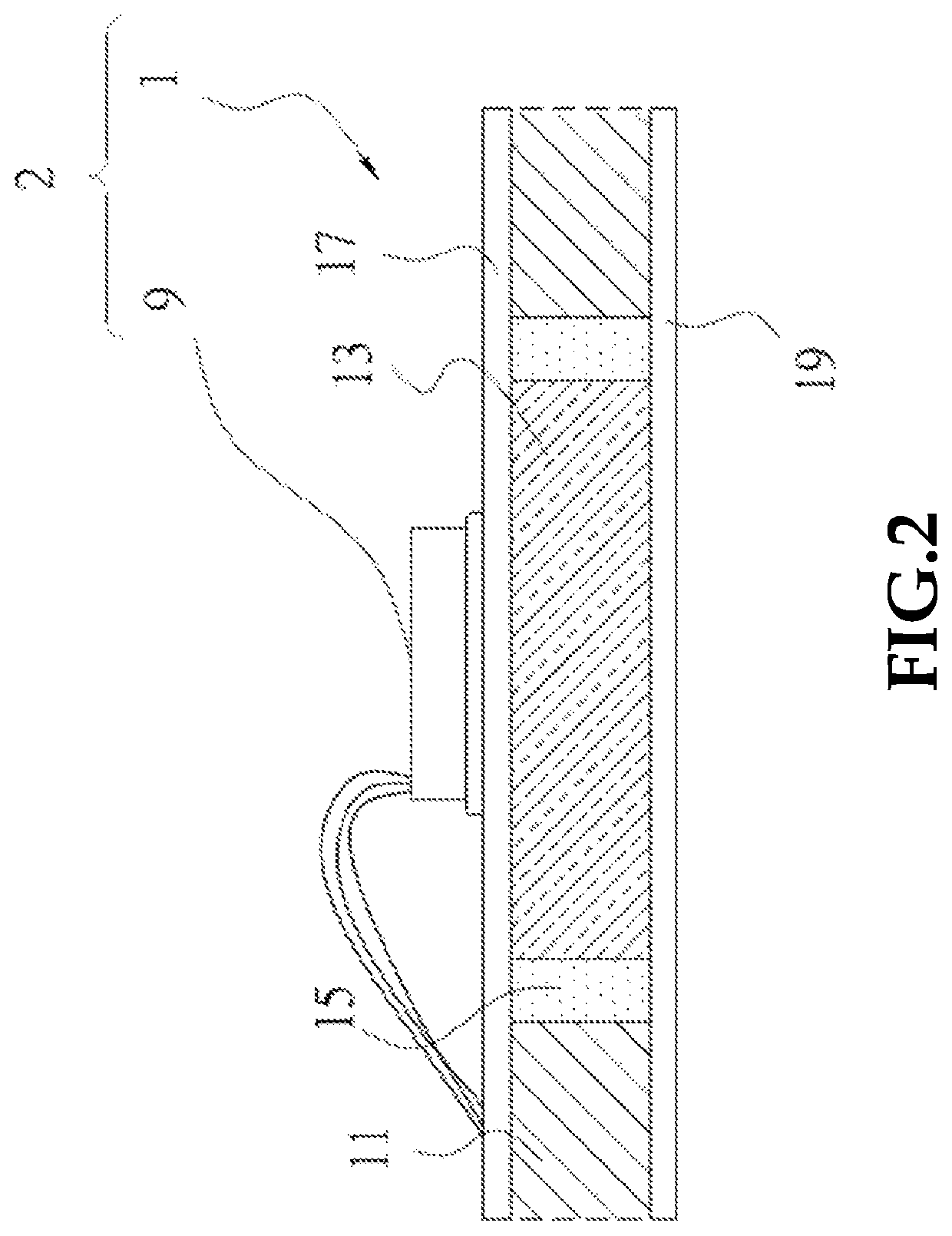
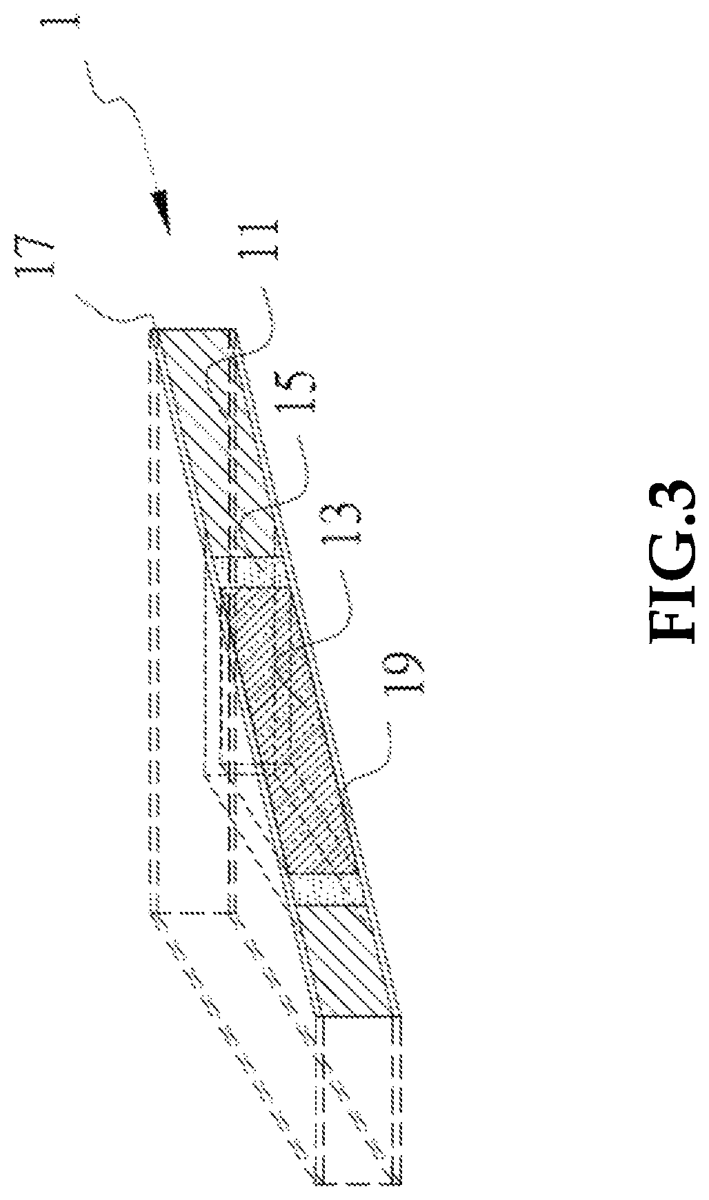
[0029]The foregoing and other technical contents, features and advantages of the present invention will be illustrated in detail by way of exemplary embodiments with reference to the accompanying drawings. In the exemplary embodiments, same elements will be indicated by similar numerals or labels.

[0030]Referring to FIGS. 2 through 5, a printed circuit board 1 with a built-in vertical heat dissipation ceramic block 13 and an electrical assembly 2 according to a first embodiment of the present invention is shown. The printed circuit board 1 includes a dielectric material layer 11, which can be obtained from a multi-layered FR-4 substrate (10 cm in both length and width). The dielectric material layer 11 defines a rectangular through hole 115 (2 cm in both length and width), which can be cut thorough laser technology. A cubic heat dissipation ceramic block 13, made of aluminum oxide (Al2O3), can be inserted in the through hole 115. However, those skilled in the art can easily understan...


PUM

PropertyMeasurementUnit
areaaaaaaaaaaa
areaaaaaaaaaaa
thermal conductivityaaaaaaaaaa

Abstract

A printed circuit board with built-in vertical heat dissipation ceramic block, and an electrical assembly are disclosed. The electrical assembly includes the board and a plurality of electronic components. The printed circuit boards includes a dielectric material layer defining at least one through hole, at least one ceramic block corresponding to the through hole, at least one fixing portion for joining the ceramic block to the through hole of the dielectric material layer, a metal circuit layer provided on upper surfaces of the dielectric material layer and the ceramic block, and a high thermal conductivity layer provided on lower surfaces of the dielectric material layer and the ceramic block. The printed circuit board allows the location and size of the ceramic block to be modified according to requirements, so as to implement complicated circuit designs, achieve good effect of thermal conduction, control thermal conduction path, and reduce manufacturing cost.

Description

FIELD OF THE INVENTION[0001]The present invention relates to a printed circuit board and, more particularly, to a printed circuit board with built-in vertical heat dissipation ceramic block, and an electrical assembly including the board.BACKGROUND OF THE INVENTION[0002]A printed circuit board (PCB) is a copper-clad substrate, which serves as a foundation for installing electronic components thereon. Generally, a copper-clad substrate includes at least one insulation layer made of a dielectric material, and a conductive layer made of copper foil and arranged on the insulation layer for forming traces (copper conductors). An insulation layer is mostly made of paper, bakelite, fiberglass, rubber, and other types of insulated material impregnated with resin. For convenience of description hereinafter, the insulation layer used in a copper-clad substrate is referred to as a dielectric material layer in the present invention.[0003]With the increasingly complex and diverse circuit design ...

Claims


Application Information

Patent Timeline
Patent Type & Authority Patents(United States)
IPC IPC(8): H05K1/02H05K1/18H01L23/367H01L23/373H05K1/03F21V29/76H01L33/64F21V29/503F21S8/08F21Y115/10
CPCH05K1/0204H05K1/0306H01L23/3731H01L23/3677H05K1/181H01L33/647H05K1/028F21Y2115/10F21V29/503H05K2201/10416H05K2201/0187F21V29/763F21S8/085H01L2224/73265H01L33/641H05K2201/10106H01L2224/48091H05K2201/068H01L2924/00014H05K2201/10166
Inventor YU, HO-CHIEHLIAO, CHENG-LUNGLIN, CHUN-YUHUANG, JASON AN-CHENG
Owner ICP TECH
Why Eureka
Try Eureka