Charged particle beam writing apparatus and method thereof

Active Publication Date: 2011-02-10
NUFLARE TECH INC
View PDF6 Cites 25 Cited by
  • Summary
  • Abstract
  • Description
  • Claims
  • Application Information

AI Technical Summary

Problems solved by technology

The position displacement caused by this charging phenomenon has not been conventionally regarded as a problem in the variable-shaped type electron beam pattern writing apparatus.
However, with the pattern miniaturization as mentioned above, such position displacement due to the charging phenomenon has become a problem.
However, since the charge dissipation layer basically has acid property, it has a poor affinity for a chemically amplified resist.
Further, there is a need to provide new equipment in order to form the charge dissipation layer, thereby increasing the m

Method used


Image

  • Charged particle beam writing apparatus and method thereof
  • Charged particle beam writing apparatus and method thereof
  • Charged particle beam writing apparatus and method thereof

Examples


embodiment 1

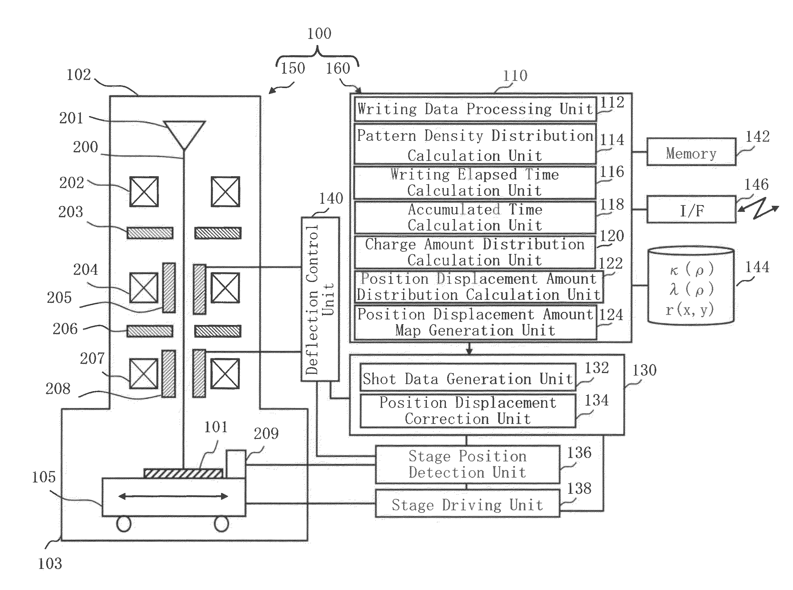
[0100]FIG. 1 is a schematic diagram showing an example of the main structure of a writing apparatus according to Embodiment 1. In FIG. 1, a writing apparatus 100 includes a writing unit 150 and a control unit 160. The writing apparatus 100 is an example of a charged particle beam writing apparatus. The writing unit 150 includes an electron lens barrel 102 and a writing chamber 103. In the electron lens barrel 102, there are arranged an electron gun assembly 201, an illumination lens 202, a first aperture plate 203, a projection lens 204, a deflector 205, a second aperture plate 206, an objective lens 207, and a deflector 208. In the writing chamber 103, there is arranged an XY stage 105, on which a target workpiece 101 serving as a writing object is placed. The target workpiece 101 is, for example, a photomask used for exposure in semiconductor manufacturing and a wafer for forming a semiconductor device. The photomask may be a mask blank where no patterns are formed. It should be u...

embodiment 2

[0149]As described in Embodiment 1, there exist position displacement caused by charge which does not change temporally and position displacement caused by temporal charge decay, and a configuration for correcting the position displacement due to temporal charge decay has been explained. In Embodiment 2, there will be described another configuration capable of further correcting position displacement due to charge which does not change temporally by using a predetermined model. Hereafter, the contents that are not especially explained are the same as those in Embodiment 1.

[0150]According to the writing apparatus described in the Patent Literature 1 mentioned above, assuming that there exists a linearly proportional relationship between an irradiation amount distribution and a charge amount distribution, a position displacement amount distribution is calculated from the irradiation amount distribution through a linear response function.

[0151]However, according to examination performe...


PUM


Abstract

A charged particle beam writing apparatus includes a charge amount distribution calculation unit configured to calculate a charge amount distribution which is charged by irradiation of a charged particle beam onto a writing region of a target workpiece, by using a charge decay amount and a charge decay time constant both of which depend on a pattern area density, a position displacement amount distribution calculation unit configured to calculate a position displacement amount of each writing position due to charge amounts of the charge amount distribution by performing convolution of each charge amount of the charge amount distribution with a response function, and a writing unit configured to write a pattern on the each writing position where the position displacement amount has been corrected, using a charged particle beam.

Description

CROSS-REFERENCE TO RELATED APPLICATION[0001]This application is based upon and claims the benefit of priority from the prior Japanese Patent Application No. 2009-184124 filed on Aug. 7, 2009 in Japan, the entire contents of which are incorporated herein by reference.BACKGROUND OF THE INVENTION[0002]1. Field of the Invention[0003]The present invention relates to a charged particle beam writing apparatus and a charged particle beam writing method. For example, it relates to an electron beam writing apparatus for writing a pattern onto a target workpiece by using a variable shaped electron beam, and to a method thereof.[0004]2. Description of Related Art[0005]The microlithography technique which advances microminiaturization of semiconductor devices is extremely important as being the unique process whereby patterns are formed in the semiconductor manufacturing. In recent years, with the high integration of LSI, the line width (critical dimension) required for semiconductor device circ...

Claims


Application Information

Patent Timeline
IPC IPC(8): H01J37/304
CPCB82Y10/00B82Y40/00H01J2237/31796H01J37/3174H01J2237/31776H01J37/3026
Inventor NAKAYAMADA, NORIAKIWAKE, SEIJI
Owner NUFLARE TECH INC
Why Eureka
Try Eureka