

Integrated circuit (IC) having tsvs with dielectric crack suppression structures
a dielectric crack and integrated circuit technology, applied in the direction of electrical apparatus, semiconductor devices, semiconductor/solid-state device details, etc., can solve the problems of significant thermally induced stress in silicon, cracking of semiconductor materials, and degrading transistor performance, so as to reduce the amount of dielectric, reduce the tsv resistance, and reduce the effect of dielectri
- Summary
- Abstract
- Description
- Claims
- Application Information
AI Technical Summary
Benefits of technology
Problems solved by technology
Method used
Image

Examples
Embodiment Construction
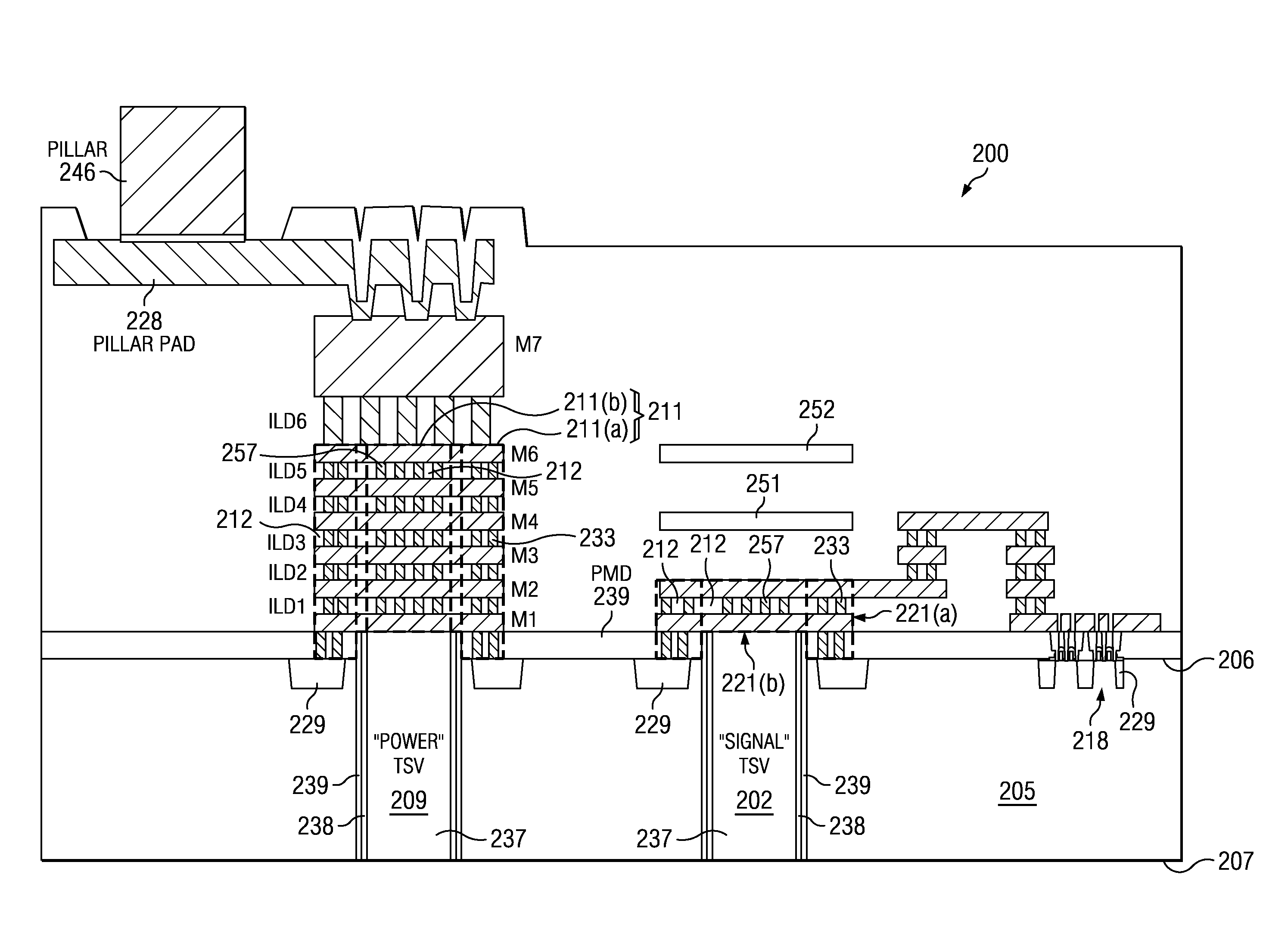
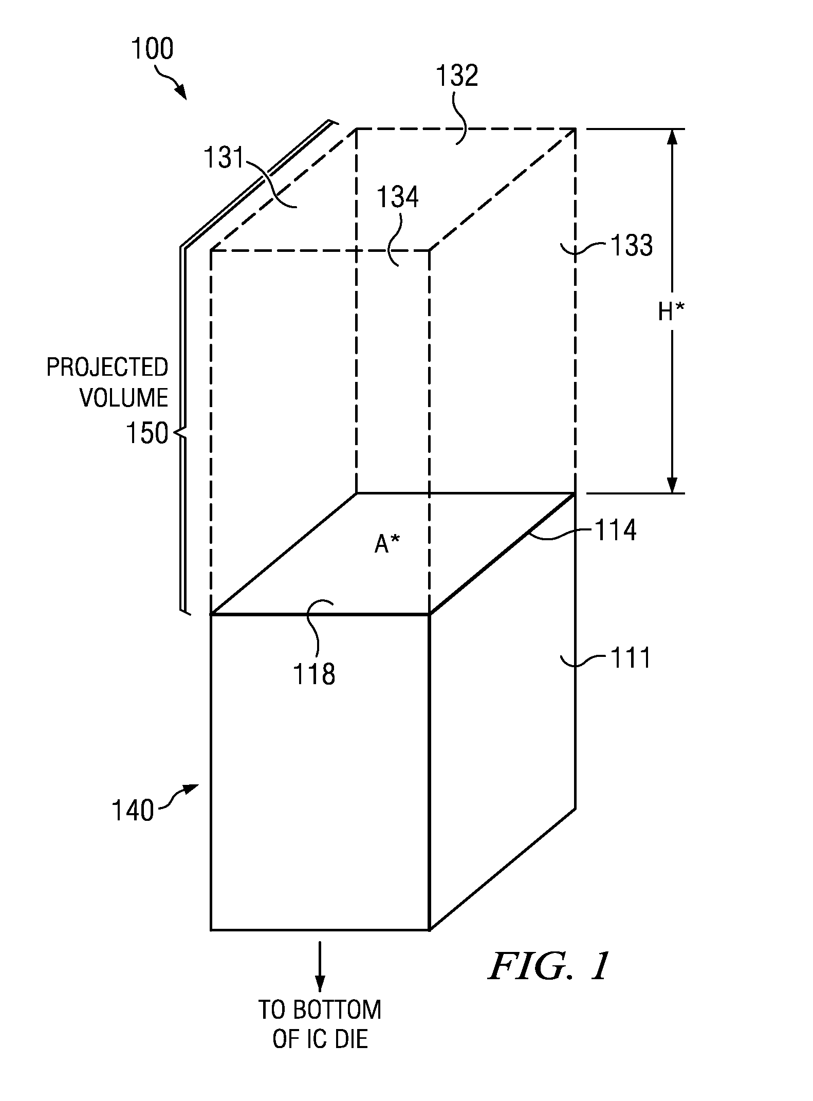
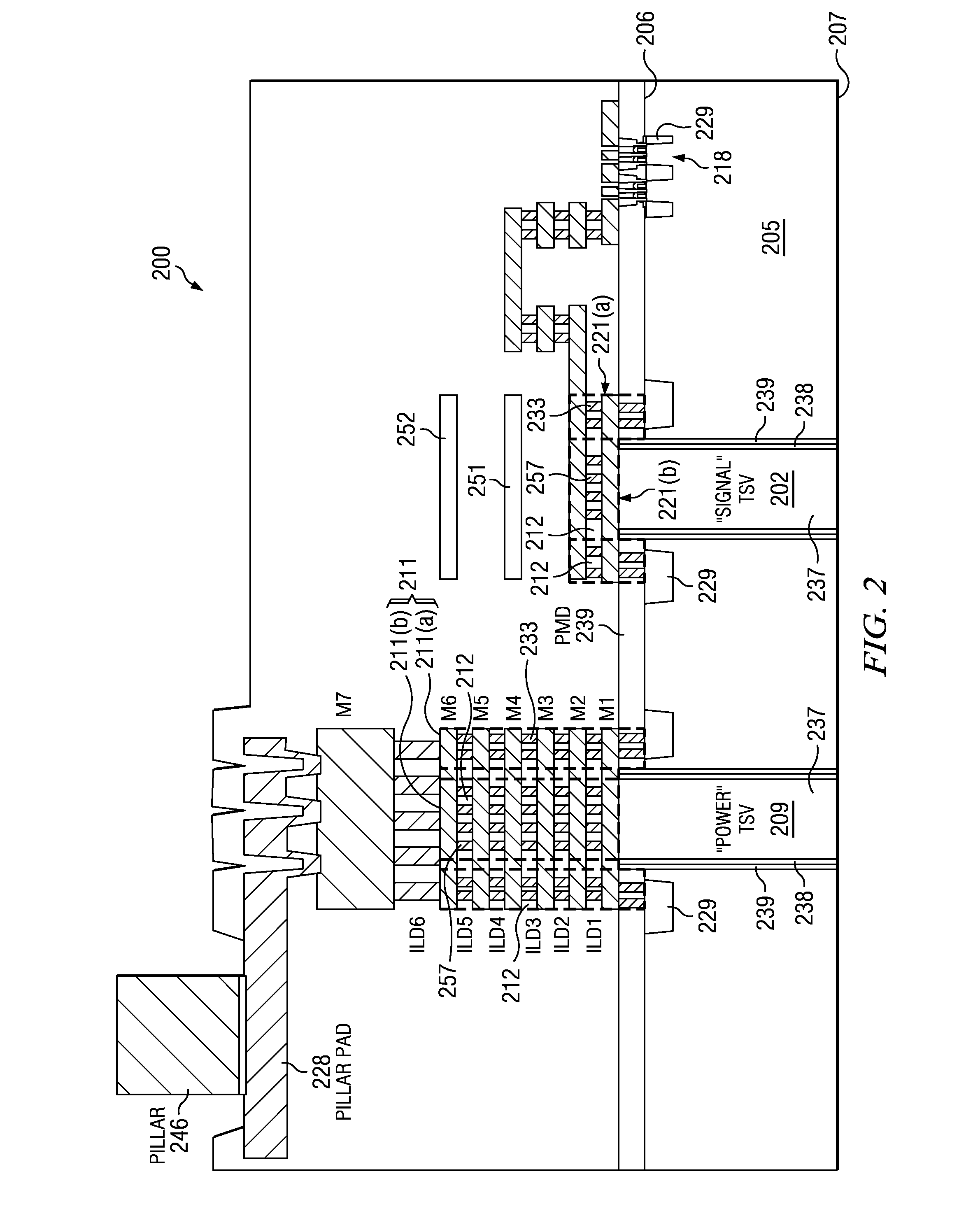
[0021]Disclosed embodiments are described with reference to the attached figures, wherein like reference numerals are used throughout the figures to designate similar or equivalent elements. The figures are not drawn to scale and they are provided merely to illustrate the disclosed embodiments. Several aspects are described below with reference to example applications for illustration. It should be understood that numerous specific details, relationships, and methods are set forth to provide a full understanding of the disclosed embodiments. One having ordinary skill in the relevant art, however, will readily recognize that the disclosed embodiments can be practiced without one or more of the specific details or with other methods. In other instances, well-known structures or operations are not shown in detail to avoid obscuring the disclosed embodiments. The disclosed embodiments are not limited by the illustrated ordering of acts or events, as some acts may occur in different orde...
PUM
 Abstract
Description
Claims
Application Information