Film capacitor and method of producing the same

Inactive Publication Date: 2011-02-10
KOJIMA PRESS IND CO LTD
View PDF9 Cites 10 Cited by
  • Summary
  • Abstract
  • Description
  • Claims
  • Application Information

AI Technical Summary

Benefits of technology

[0038]In addition, the film capacitor of the present invention is free from a problem of deterioration of the withstand voltage caused by the influence of impurities in material of the resin film layer, because the thickness of the resin film layer is not excessively reduced. Further, when the vapor-deposited metal film layer is continuously formed on the resin film layer by metal deposition, the occurrence of wrinkles on the resin film layer by high-speed winding can be prevented. Furthermore, the resin film layer may not be thermally affected, when metal atoms having high-temperatures are attached to the resin film layer in the metal deposition process.
[0039]In the stacked and wound film capacitors of the present invention, even if the vapor-deposited polymer film layer is formed on the resin film layer, which is one of the dielectric layers, the thickness of the vapor-deposited polymer film layer and impurities in the film are sufficiently reduced. As a result, both of dielectric constant and withstand voltage of the vapor-deposited polymer film layer are sufficiently improved. In addition, the vapor-deposited polymer film layer has a uniform thickness, so that the surface smoothn

Problems solved by technology

However, when the thickness of the resin film is reduced, influence of impurities (residue) in the film materials becomes bigger, resulting in deterioration of withstand voltage of the resin film.
For that reason, there is a limitation on a reduction in thickness of the resin film.
Thus, in the film capacitor having a conventional structure, only by reducing the thickness

Method used


Image

  • Film capacitor and method of producing the same
  • Film capacitor and method of producing the same
  • Film capacitor and method of producing the same

Examples


Embodiment Construction

[0065]To further clarify the present invention, there will be described in detail embodiments of the present invention with reference to the accompanying drawings.

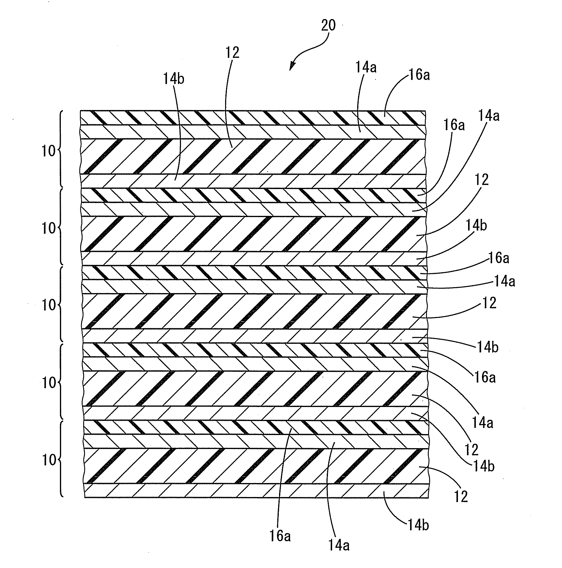
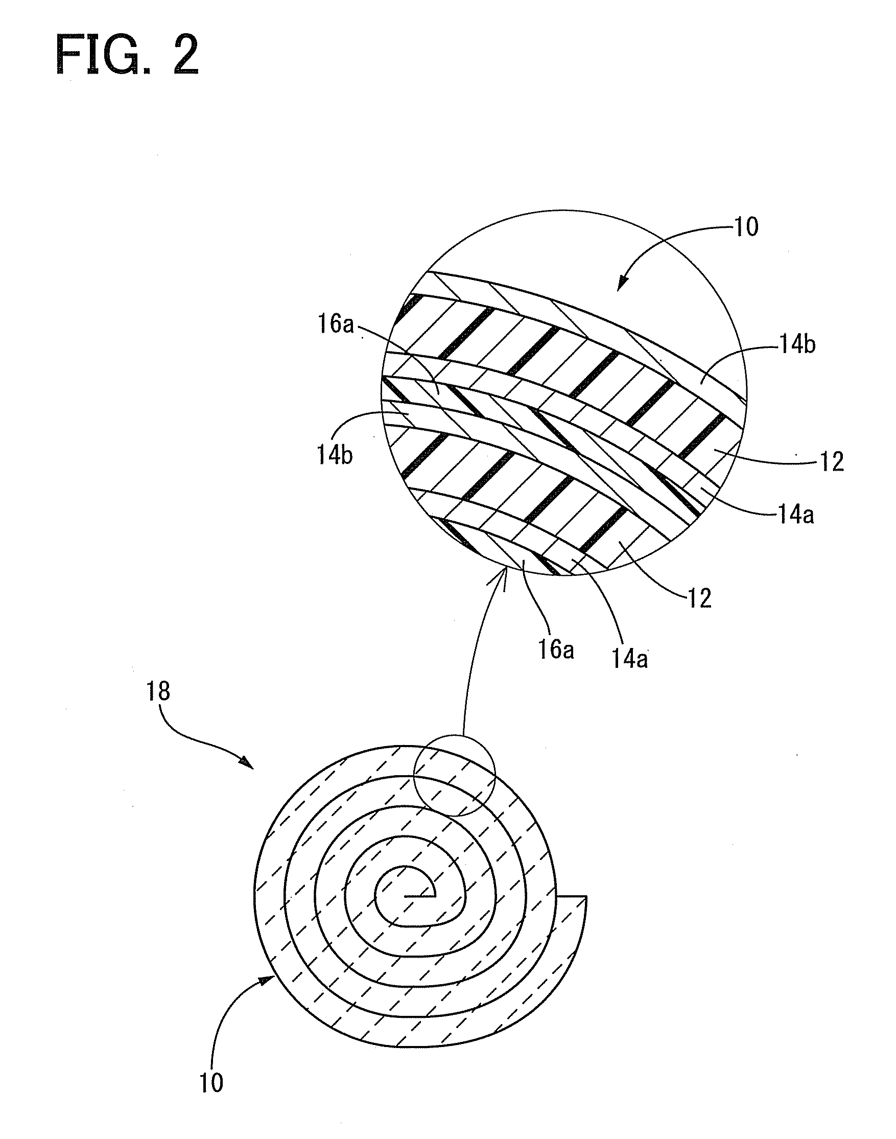
[0066]Initially, FIG. 1 shows an example of a multilayer film constituting a basic element, which is a component of a film capacitor according to the present invention, in a state in which the multilayer film is not wound. As apparent from FIG. 1, a multilayer film 10 having a sheet shape includes a resin film 12 as a dielectric, which constitutes one dielectric layer of a multilayer structure. Here, the resin film 12 is formed of a stretched film made of polypropylene and has a thickness of about 1 to 10 μm. However, the material of the resin film 12 is not particularly limited to polypropylene. Instead of polypropylene, resin materials such as polyethylene terephthalate, polyphenylene sulfide, polyethylene naphtalate and the like, which are used as materials of resin films of conventional film capacitors, can be suitably...


PUM

PropertyMeasurementUnit
Thicknessaaaaaaaaaa
Thicknessaaaaaaaaaa
Structureaaaaaaaaaa

Abstract

A film capacitor is provided which has a smaller size and improved capacity while securing a sufficient withstand voltage. The film capacitor comprising a basic element 10 containing a plurality of dielectric layers and at least one vapor-deposited metal film layer 14a, 14b, where the plurality of dielectric layers consisting of a resin film layer 12 and at least one vapor-deposited polymer film layer 16a, and the at least one vapor-deposited polymer film layer 16a is formed on at least one of the resin film layer 12 and the at least one vapor-deposited metal film layer 14a, 14.

Description

[0001]The present application is based on Japanese Patent Applications No. 2009-185421 filed on Aug. 10, 2009 and No. 2010-021714 filed on Feb. 3, 2010, the contents of which are incorporated herein by reference.BACKGROUND OF THE INVENTION[0002]1. Field of the Invention[0003]The present invention relates to a film capacitor. More particularly, the present invention relates to an improvement of a wound film capacitor and a stacked film capacitor.[0004]2. Discussion of Related Art[0005]Conventionally, as one type of film capacitor for use in an electric device, there are known a wound film capacitor and a stacked film capacitor. As disclosed in JP-A-2007-220720, the wound film capacitor is generally produced by winding a multilayer film (metallized film) in which a vapor-deposited metal film (layer) as an electrode film is formed by a vacuum deposition method on one surface of a dielectric (layer) consisting of a resin film (layer) having insulating properties, which is formed of poly...

Claims


Application Information

Patent Timeline
IPC IPC(8): H01G4/30H01G4/18B32B37/02B65H18/00
CPCH01G4/145H01G4/33H01G4/32H01G4/306
Inventor ITO, KAORUNOGUCHI, MASUMI
Owner KOJIMA PRESS IND CO LTD
Why Eureka
Try Eureka