Nano-tube thermal interface structure

Active Publication Date: 2011-02-10
RAYTHEON CO
View PDF13 Cites 33 Cited by
  • Summary
  • Abstract
  • Description
  • Claims
  • Application Information

AI Technical Summary

Benefits of technology

3. CNT-foil structures are sandwiched between the semiconductor and heat sink to minimize application time and maximize reworkability
With such an arrangement, a Nano-Thermal Interface Material (nTIM) uses metallic bonding materials to attach high-performance Carbon Nano-Tube (CNT)-foil carriers to device and heat sink interfaces. This minimizes joint resistances through optimization of thin metallic bonds and multi-walled carbon nanotube (MWCNT) arrays grown on foils, providing a “drop-in” TIM solution that does not require modification to either the semiconductor device or heat sink. The CNT-foil interposers comply with micro-rough heat sink surfaces t

Problems solved by technology

However, they are susceptible to thermal fatigue and aging, are not always easily reworkable, and may transfer large stresses to the die which limits die thinning concepts.
673, 1998); however, both multi-(MW) and single-walled (SW) CNTs have yet to reach their potential in interface applications.
While possessing greater theoretical conductivity, SWCNTs are problematic in vertically aligned array interface app

Method used


Image

  • Nano-tube thermal interface structure
  • Nano-tube thermal interface structure
  • Nano-tube thermal interface structure

Examples


Embodiment Construction

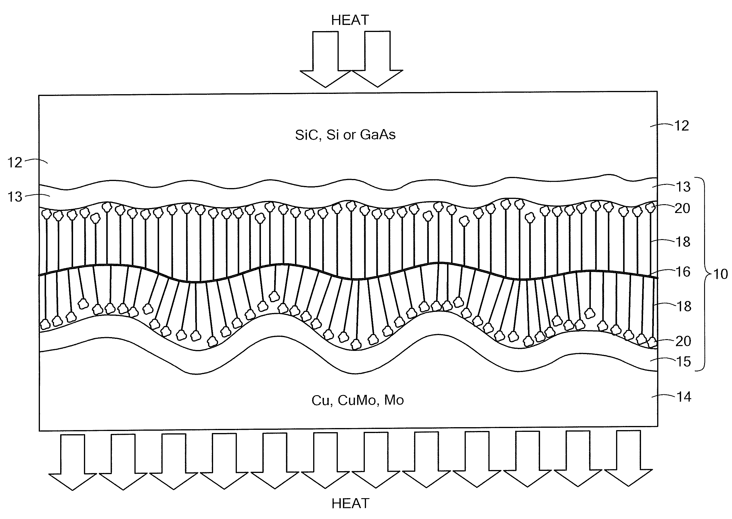
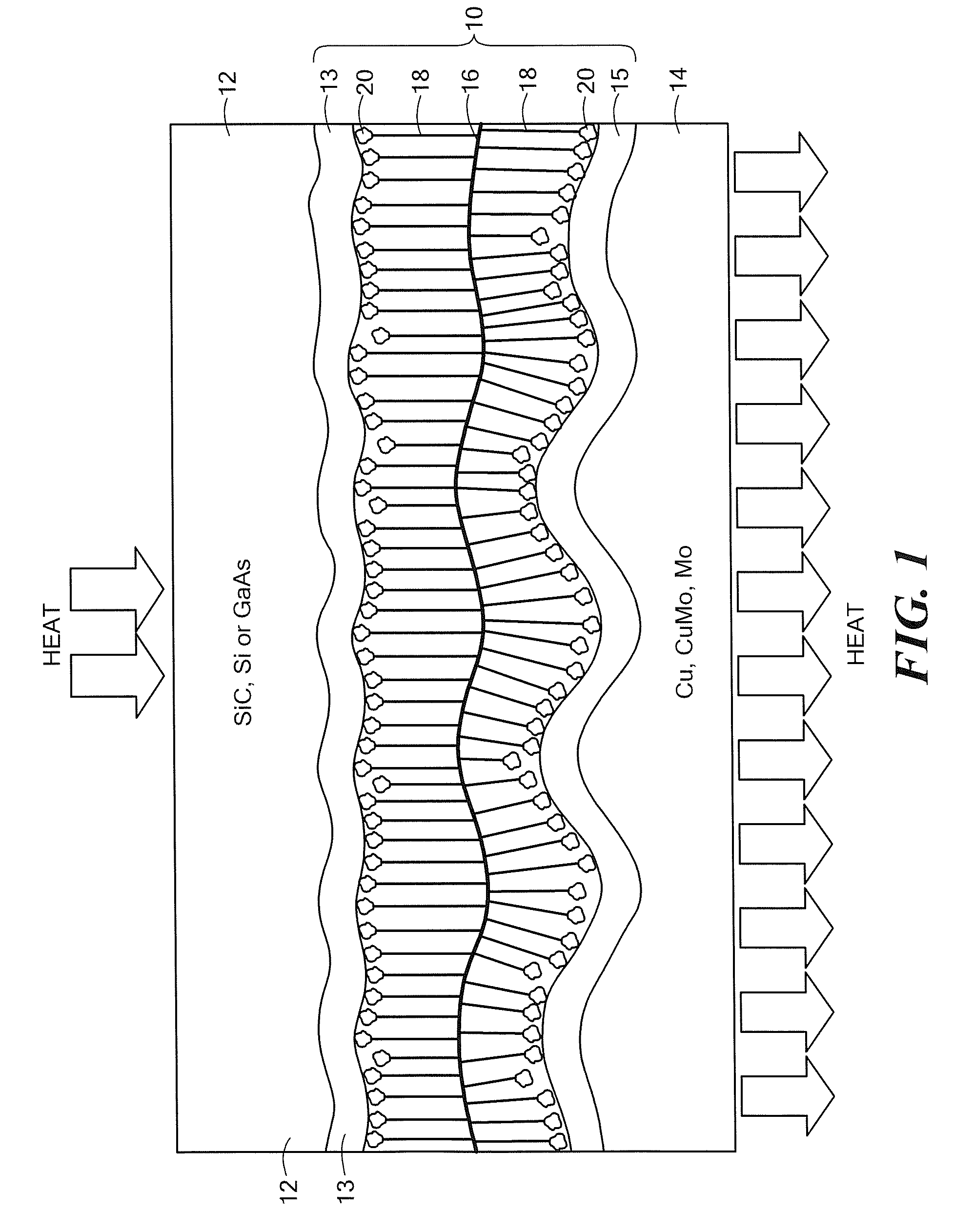
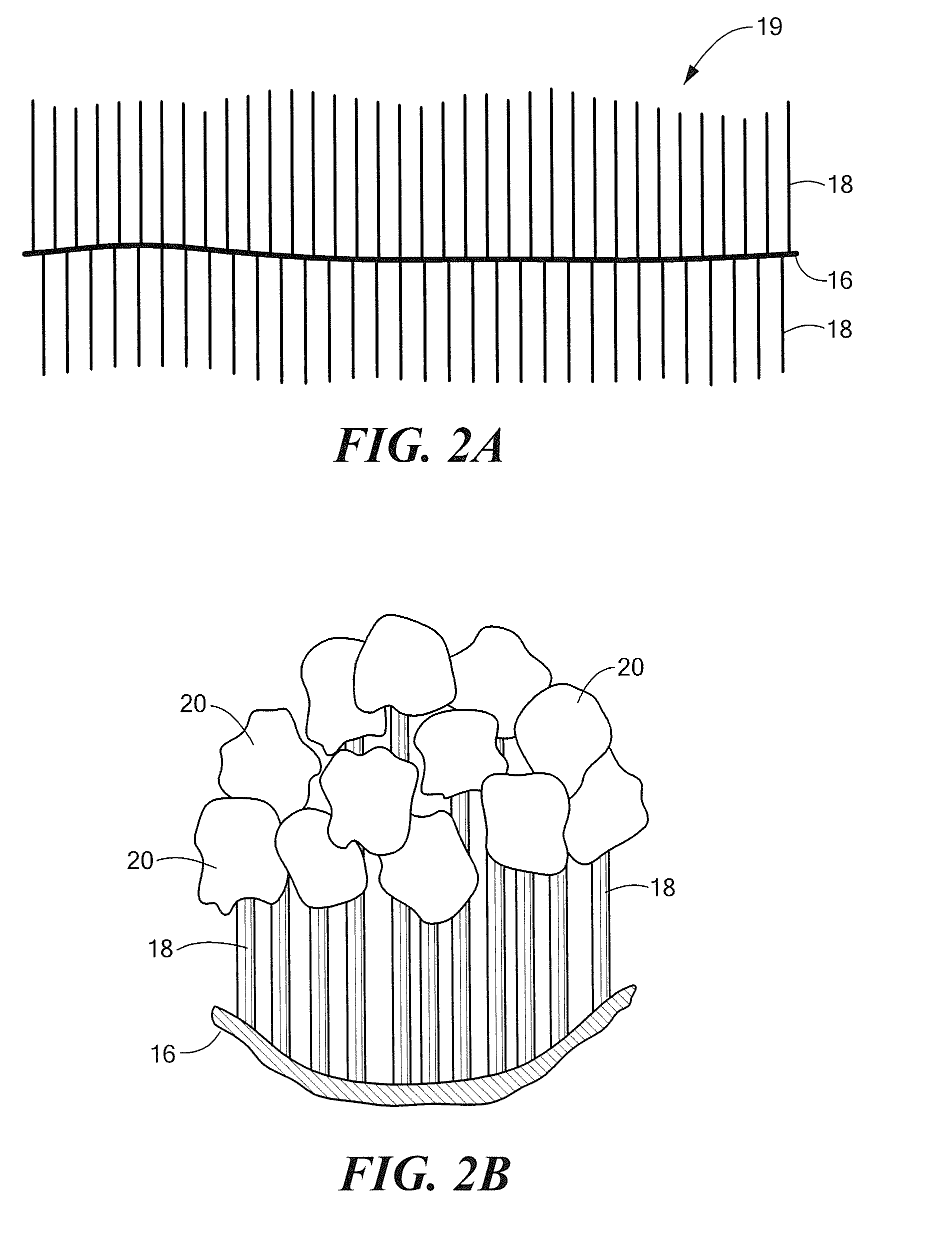
Referring to FIG. 1, a structure 10 is used to transport heat generated in a heat source 12, here a monolithic microwave integrated circuit (MMIC) 12 having a metal ground plane conductor layer 13, here a thermally and electrically conductive material such as, for example, Ti / Au or W / Au, on the bottom surface of the chip 12 to a conductive layer 15, here for example, of the same material as the layer 13, on the upper surface of a heat sink 14. The structure 10 includes a electrically and thermally conductive carrier layer 16 having high lateral thermal spreading properties (such as copper or aluminum; here preferably graphene or graphene-based materials such as pure graphene films, interwoven-CNT films and exfoliated graphite papers). The carrier layer 16 has directly grown on upper and lower surfaces thereof a plurality of generally vertically extending the hollow nano-tubes 18 here using microwave plasma chemical vapor deposition or thermal chemical vapor deposition.

The nano-tubes...


PUM


Abstract

A structure, comprising: a semiconductor structure having an electrically and thermally conductive layer disposed on one surface of the semiconductor structure; an electrically and thermally conductive heat sink; a electrically and thermally conductive carrier layer; a plurality of electrically and thermally nano-tubes, a first portion of the plurality of nano-tubes having proximal ends disposed on a first surface of the carrier layer and a second portion of the plurality of nano-tubes having proximal ends disposed on an opposite surface of the carrier layer; and a plurality of electrically and thermally conductive heat conductive tips disposed on distal ends of the plurality of nano-tubes, the plurality of heat conductive tips on the first portion of the plurality of nano-tubes being attached to the conductive layer, the plurality of heat conductive tips on the second portion of the plurality of nano-tubes being attached to the heat sink.

Description

TECHNICAL FIELDThis disclosure relates generally to thermal interface structures and more particularly to nano-tube thermal interface structures.BACKGROUNDAs is known in the art, in many applications it is necessary to remove heat from, for example, microelectronic components such as semiconductor integrated circuit chips. One heat removal or, more generally, thermal management technique, includes the use of a thermal interface structure disposed between the integrated circuit chip and a heat sink,As is also known in the art, the trend of increasing power density in microelectronic components has accelerated the need for improved thermal management techniques. With heat fluxes ranging from 0.1-3 kW / cm2 being expected in next generation silicon and wide band gap semiconductor electronics, reducing thermal resistances across interfaces has become crucial in reducing device operational temperature and ensuring reliability. This research challenge has led to the development of new therm...

Claims


Application Information

Patent Timeline
IPC IPC(8): H05K7/20H01L21/60
CPCH01L23/373Y10T428/2938H01L23/3733H01L23/3737Y10S977/742Y10S977/762Y10S977/832Y10S977/72H01L2924/0002H01L23/433Y10T428/2958Y10T428/25Y10T428/2918H01L2924/00
Inventor ALTMAN, DAVID H.NORDHAUSEN, ERIK F.BERNSTEIN, STEVEN D.MOLFINO, ROBERT P.WAKEFIELD, STEVEN B.
Owner RAYTHEON CO
Why Eureka
Try Eureka