Doping method, and method for producing semiconductor device

a technology of semiconductor devices and impurities, which is applied in the direction of semiconductor devices, basic electric elements, electrical appliances, etc., can solve the problems of property degradation of the semiconductor layer, difficult to obtain the desired properties of the semiconductor device, and the above-mentioned doping methods to control the concentration of impurities used to dope the semiconductor layer. achieve the effect of high accuracy and well-controlled properties

Inactive Publication Date: 2011-02-10
SONY CORP
View PDF2 Cites 8 Cited by
  • Summary
  • Abstract
  • Description
  • Claims
  • Application Information

AI Technical Summary

Benefits of technology

[0007]Thus, there is a need for a doping method compatible with a vacuumless (large-area processible), low-temperature process, which also allows the impurity concentration to be controlled with high accuracy without losing the semiconductor properties. There also is a need for a production method capable of providing a semiconductor device with well controlled property accuracy.
[0010]In accordance with such a method, antimony is diffused from the antimony compound layer containing elements selected from the group consisting of hydrogen, nitrogen, oxygen, and carbon, and antimony. Therefore, antimony can be diffused into the substrate without losing the properties of the substrate (semiconductor properties). Further, as described later in Examples, it has been confirmed that this method allows the substrate to be doped with antimony at a high concentration corresponding well to the antimony concentration of the material solution. Further, the heat treatment for diffusing antimony into the substrate is performed by energy beam irradiation. The method is thus compatible with a low-temperature process.
[0011]As described above, the doping method according to the embodiment of the invention is compatible with a vacuumless, low-temperature process, and also allows the impurity doping concentration to be controlled with high accuracy without losing the semiconductor properties. Further, use of such a method makes it possible to provide a semiconductor device with well controlled properties.

Problems solved by technology

However, it is difficult for the above doping methods to control the concentration of impurities used to dope the semiconductor layer.
In the first example, silicon oxide in the silicate glass forming PSG or BSG is also taken into the semiconductor layer, resulting in property degradation of the semiconductor layer.
Further, the second example does not allow high-concentration phosphorus (P) or boron (B) doping, and it thus is difficult to obtain a semiconductor device with desired properties by the above doping methods.

Method used


Image

  • Doping method, and method for producing semiconductor device
  • Doping method, and method for producing semiconductor device
  • Doping method, and method for producing semiconductor device

Examples


first embodiment

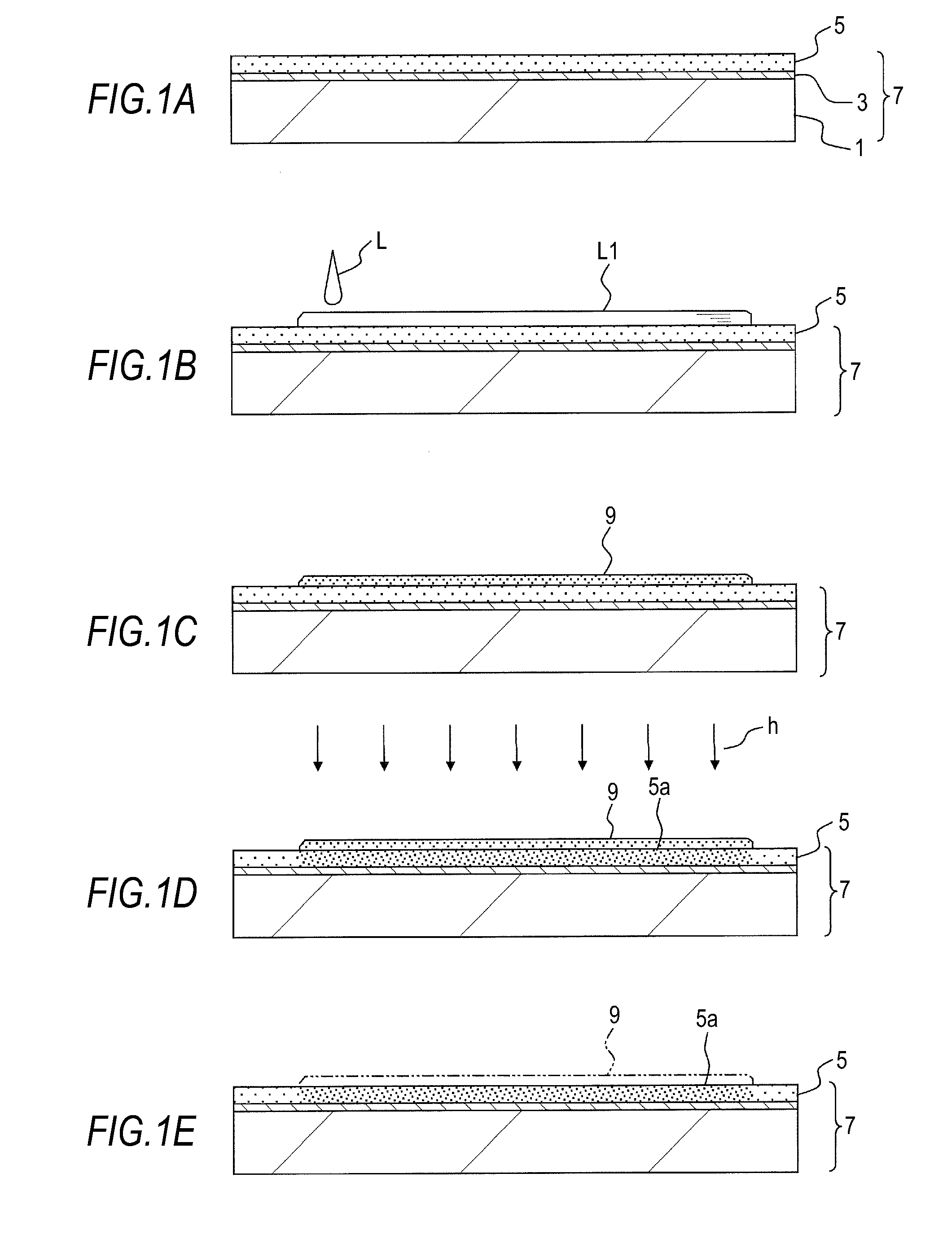
[0023]FIGS. 1A to 1E show a flow chart illustrating a doping method according to this embodiment in cross section. The following will describe the doping method based on these figures.

[0024]First, as shown in FIG. 1A, a supporting substrate 1 is prepared, and a buffer layer 3 made of an insulating material such as silicon oxide or silicon nitride is formed thereon. The supporting substrate 1 used here is a crystalline or amorphous substrate. Examples of crystalline substrates include a semiconductor substrate and a quartz substrate. Preferred examples of amorphous substrates include those that have low thermal resistance (low melting point) but allow the production of large-area substrates easily at low cost, such as those made of glass or an organic polymeric material (plastic). If necessary, the supporting substrate 1 may have flexibility.

[0025]Subsequently, a semiconductor layer 5 is formed on the supporting substrate 1 having formed thereon the buffer layer 3. The semiconductor ...

second embodiment

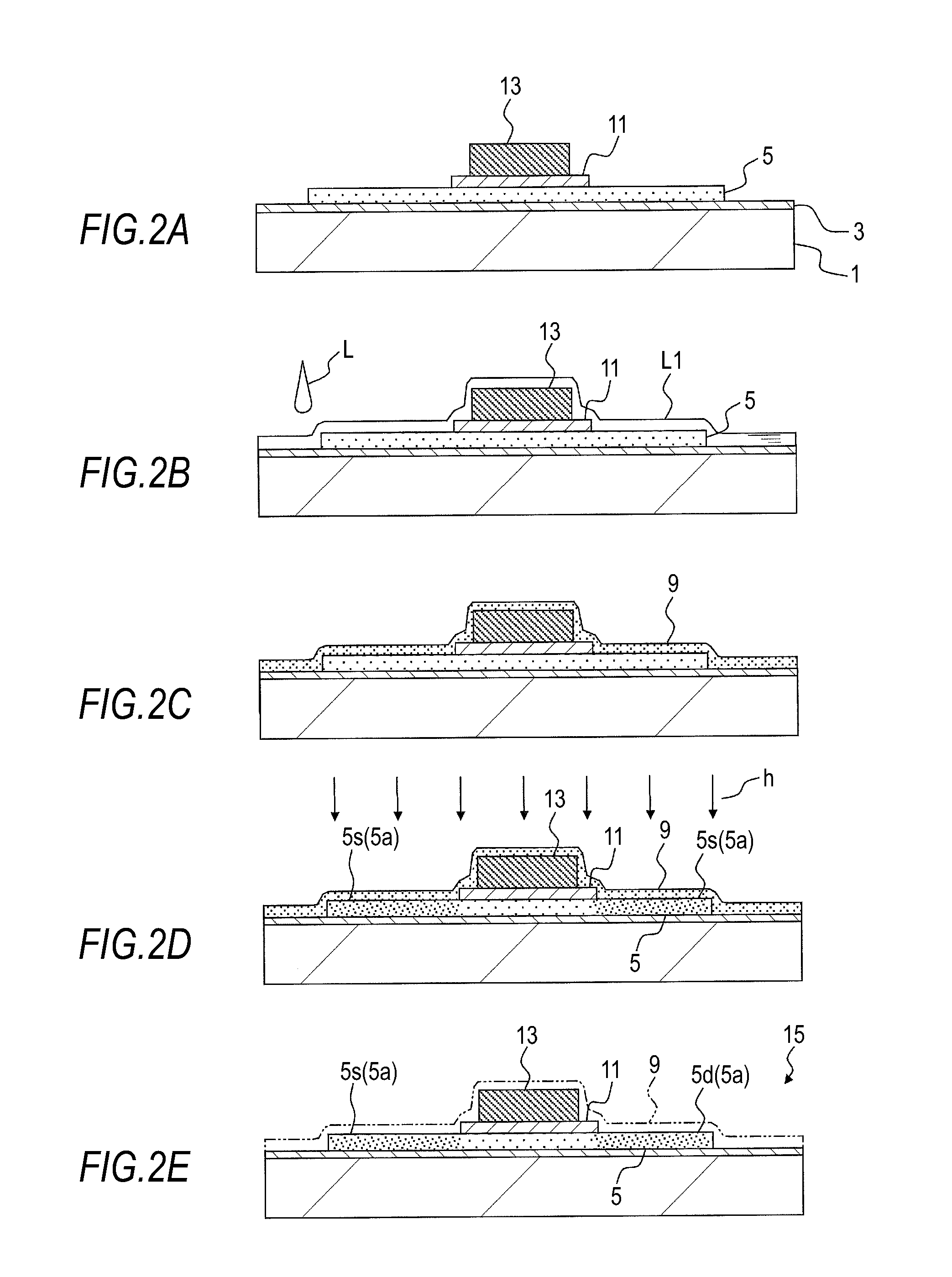
[0040]FIGS. 2A to 2E show a flow chart illustrating a method for producing a semiconductor device according to a second embodiment in cross section, which applies the doping method of the first embodiment. FIGS. 2A to 2E show the production of a semiconductor device configured as a thin-film transistor with an offset structure. The following describes the method for producing a semiconductor device based on these figures. The components common to the first embodiment are indicated with the same reference numerals, and will not be further described.

[0041]First, as shown in FIG. 2A, a semiconductor layer 5 is formed on a supporting substrate 1 with a buffer layer 3 therebetween, and, if necessary, the semiconductor layer 5 is patterned into islands and crystallized.

[0042]Next, across the semiconductor layer 5 in the form of islands, a gate insulating film 11 is formed above the supporting substrate 1 and then patterned. The gate insulating film 11 formed here is made of silicon oxide,...

third embodiment

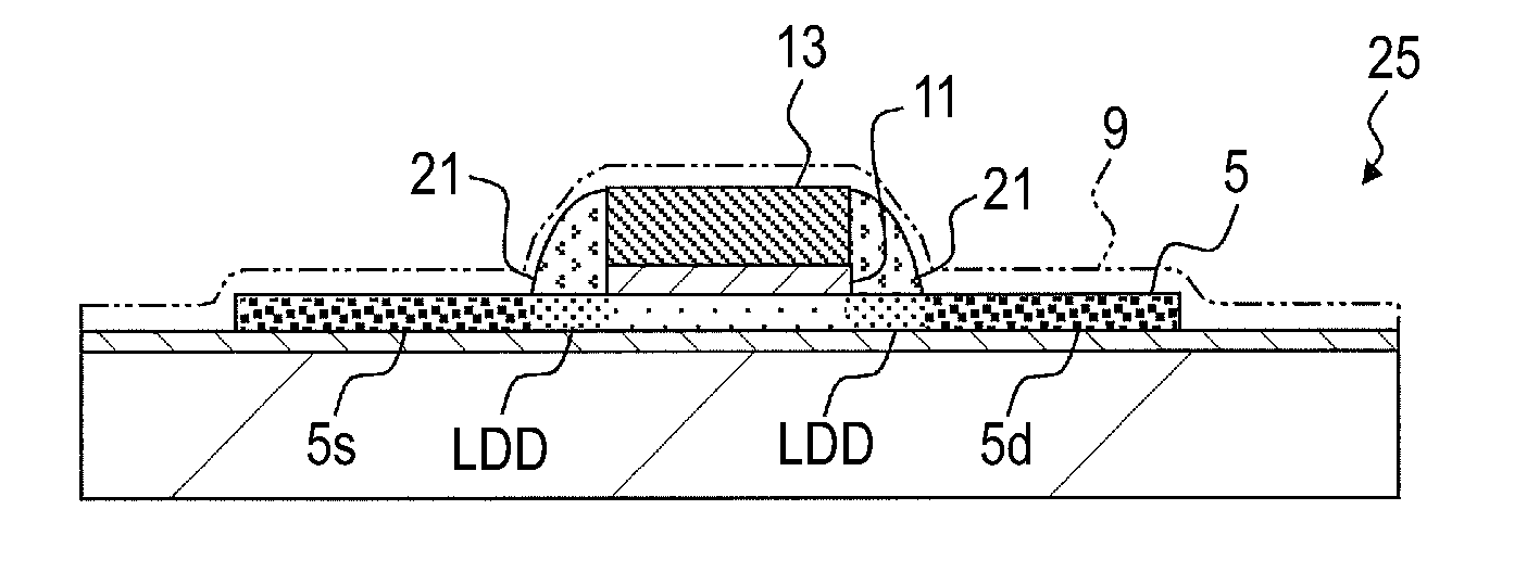
[0052]FIGS. 3A to 3E and 4A to 4E show a flow chart illustrating a method for producing a semiconductor device according to another embodiment in cross section, which applies the doping method of the first embodiment. These figures show the production of a semiconductor device configured as a thin-film transistor with a LDD structure. The following describes the method for producing a semiconductor device based on these figures. The components common to the first and second embodiments are indicated with the same reference numerals, and will not be further described.

[0053]First, as shown in FIG. 3A, a semiconductor layer 5 is formed on a supporting substrate 1 with a buffer layer 3 therebetween, and, if necessary, the semiconductor layer 5 is patterned into islands and crystallized.

[0054]Next, across the semiconductor layer 5 in the form of islands, a gate insulating film 11 and a gate electrode 13 are formed in the same pattern above the supporting substrate 1. The gate insulating ...


PUM

PropertyMeasurementUnit
thickaaaaaaaaaa
concentrationaaaaaaaaaa
semiconductoraaaaaaaaaa

Abstract

A doping method includes: a first step of depositing a material solution containing an antimony compound containing elements selected from the group consisting essentially of hydrogen, nitrogen, oxygen, and carbon together with antimony to a surface of a substrate; a second step of drying the material solution to form an antimony compound layer on the substrate; and a third step of performing heat treatment so that antimony in the antimony compound layer is diffused into the substrate.

Description

BACKGROUND OF THE INVENTION[0001]1. Field of the Invention[0002]The preset invention relates to a doping method and a method for producing a semiconductor device, and especially to a method suitable for the production of a thin-film semiconductor device.[0003]2. Description of the Related Art[0004]The use of a lightweight, flexible plastic substrate as a supporting substrate in a semiconductor device including a thin-film semiconductor layer has been considered. In the production of such a semiconductor device, in consideration of the thermal resistance of the plastic substrate, a low-temperature process is desired. Therefore, also in the impurity doping of the semiconductor layer, a method that allows impurity doping at a low temperature has been considered as a substitute for ion implantation that requires high-temperature heat treatment to remove hydrogen. Further, with the increase in the size of the substrate, existing vacuum processes almost reach a limit in terms of the size ...

Claims


Application Information

Patent Timeline
Patent Type & Authority Applications(United States)
IPC IPC(8): H01L21/336H01L21/22
CPCH01L21/2225H01L21/2254H01L29/78621H01L29/66757H01L21/2255H01L21/20
Inventor KONO, TADAHIROMACHIDA, AKIOFUJINO, TOSHIO
Owner SONY CORP
Why Eureka
Try Eureka