Multilayer wiring substrate having cavity portion

a multi-layer wiring and cavity technology, applied in the field of semiconductor chips, can solve the problems of large-sized substrates, difficult to form thinner substrates, and cracks in ceramic substrates, and achieve the effect of low reflectance and low profil

Inactive Publication Date: 2011-02-24
MITSUBISHI PLASTICS INC
View PDF5 Cites 37 Cited by
  • Summary
  • Abstract
  • Description
  • Claims
  • Application Information

AI Technical Summary

Benefits of technology

[0025]According to the present invention, (1) the multilayer wiring substrate can be compact and lower profile, thereby LED elements can be densely-mounted; (2) the multilayer wiring substrate comprises a cavity portion for mounting LED elements; (3) even a small-sized cavity portion or a complexly-shaped cavity portion can be efficiently formed; and (4) the wiring substrate exhibits extremely low decreasing rate in reflectance under high reflectance characteristics and high temperature environment. So, by mounting LED elements and so on, it is possible to provide a multilayer wiring substrate having a cavity portion which also functions as a reflector.

Problems solved by technology

When using a ceramic substrate, the problem of yellow discoloration does not happen; however, the ceramic substrate tends to be broken whereby it is difficult to produce a larger-sized substrate.
Moreover, from the aspect of substrate structure, since the glass-cloth / titanium oxide-added white bismaleimide-triazine resin and the white epoxy resin contain a glass cloth, it is difficult to form a thinner substrate, so that conventional commercially available substrates have at least about 40 μm in thickness.
In addition, ceramic substrate cannot maintain a certain mechanical strength, so that the thickness is usually about 400 μm and it is difficult to form a thinner substrate.
Because of the dam effect of the reflector, the insert forming type exhibits good workability in resin sealing, on the one hand; there still exist problems of adhesiveness between a metal frame and a resin.
When adopting spot facing, restriction of the pattern designing and scraps produced at a time of processing become the problems.

Method used


Image

  • Multilayer wiring substrate having cavity portion
  • Multilayer wiring substrate having cavity portion
  • Multilayer wiring substrate having cavity portion

Examples


example 1

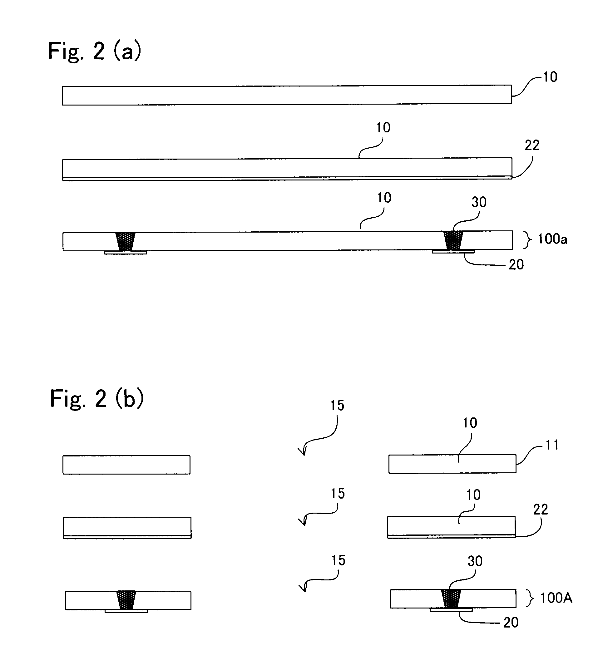
[0193](Production of the Wiring Substrate 100a)

[0194]A thermoplastic resin composition obtained by mixing: to 100 parts by mass of a resin mixture having: 40 mass % of a polyether ether ketone resin (PEEK 450G, Tm=335° C.), and 60 mass % of an amorphous polyetherimide resin (ULTEM 1000) ; 16 parts by mass of titanium oxide (average particle diameter of 0.23 μm, alumina treatment, silane coupling treatment) produced by chlorine method; and 45 parts by mass of a synthetic mica having an average particle diameter of 5 μm and an average aspect ratio of 50, was melt-kneaded, then the melt-kneaded resin composition was extruded into a film having a thickness of 100 μm simultaneously with lamination of a copper foil 22 from one side thereof, to obtain a one-sided copper-laminated insulating base material. Via holes each having a diameter of 100 μm were formed at predetermined positions using laser and a conductive paste composition was filled in the via holes by screen printing. After fill...

example 2

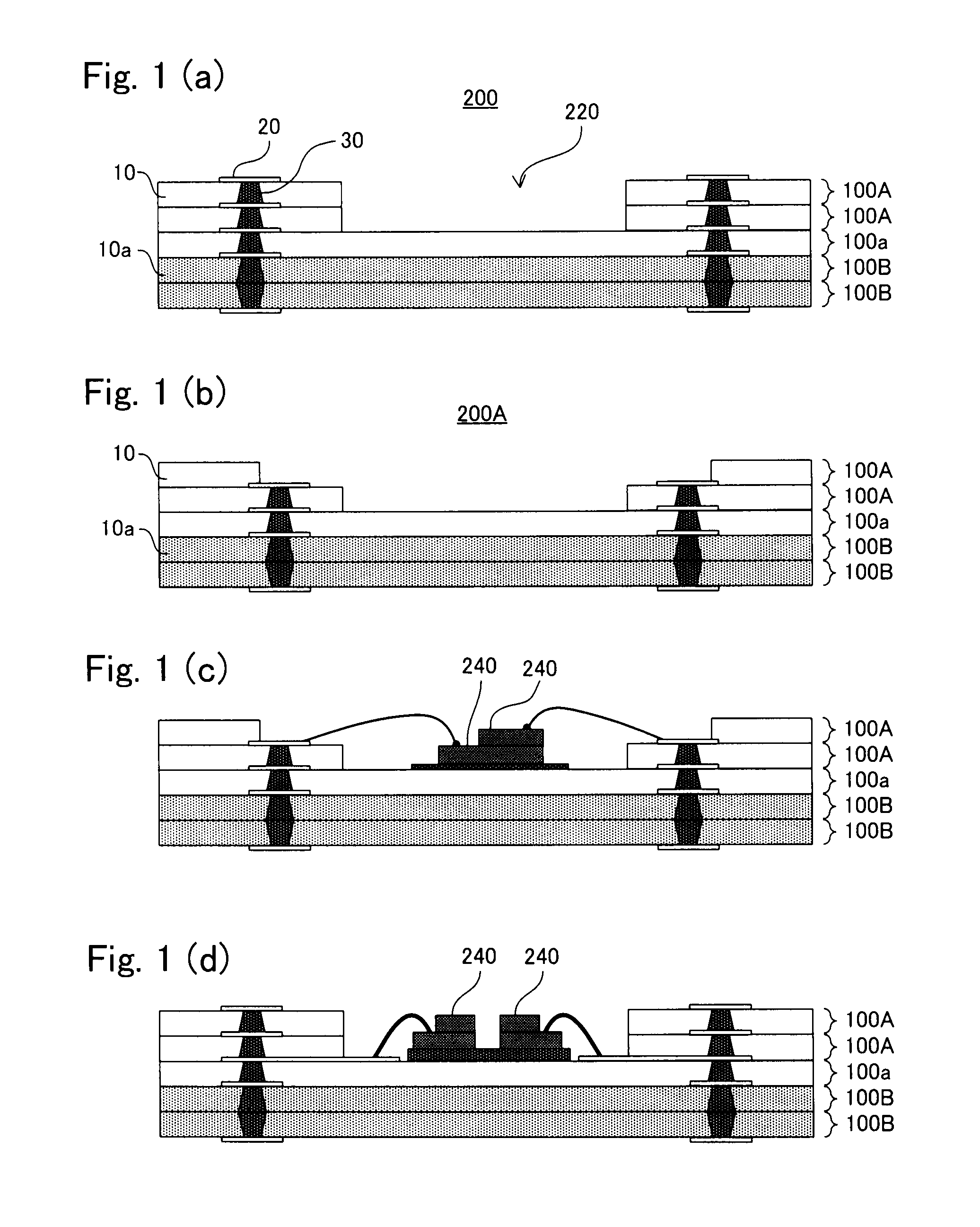
(Fabrication of the Multilayer Wiring Substrate 200A)

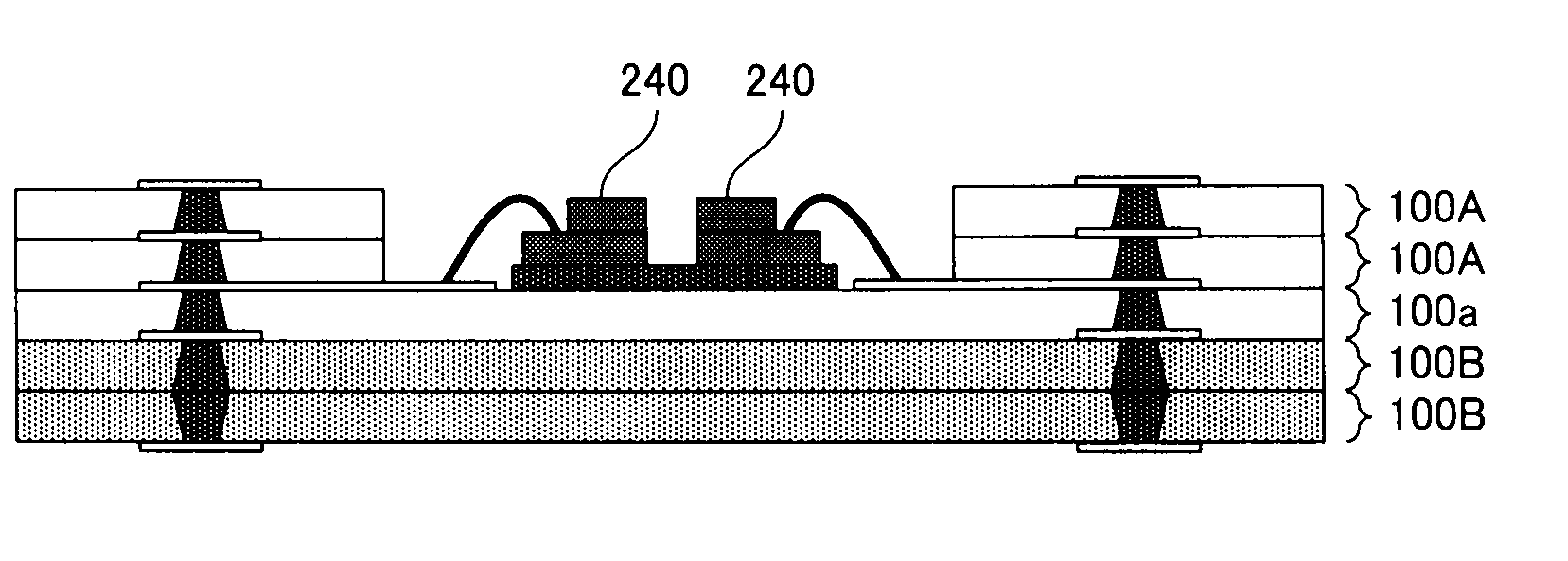
[0199]In the same manner as Example 1, the wiring substrate 100a and the wiring substrate (s) 100A were produced. With respect to the wiring substrates 100A, the first wiring substrate has a cavity hole 15 having the same size as that of Example 1 and the second one has a cavity hole 15 having slightly larger size. Thereafter, the two wiring substrates 100B were laminated at a lower side, the one wiring substrate 100a was laminated on the wiring substrates 100B along the bottom face of the cavity portion, the first wiring substrate 100A having the cavity hole 15 having the same size as that of Example 1 was laminated thereon, and finally, the second wiring substrate 100A having the cavity hole 15 having slightly larger size than that of Example 1 was laminated. By arranging a staircase-pattern polyimide resin-made spacer 260 having the same shape and thickness in the space to be the cavity portion 220, and by thermocompression bon...

example 3

(Production of the Wiring Substrate 100D)

[0200]A thermoplastic resin composition obtained by mixing: to 100 parts by mass of a resin mixture having: 65 mass % of a polyether ether ketone resin (PEEK 450G, Tm=335° C.), and 35 mass % of an amorphous polyetherimide resin (ULTEM 1000); 39 parts by mass of a synthetic mica having an average particle diameter of 5 μm and an average aspect ratio of 50, was melt-kneaded; and then the melt-kneaded resin composition was extruded into a film (i.e. insulating base material) having a thickness of 100 μm. After giving corona discharge treatment to both sides of the obtained film, a solution containing a polymerizable monomer prepared by mixing 50 mass % of dimethallyl bisphenol A and 50 mass % of bis(4-maleimidephenyl)methane was applied on a mold-releasable PET film and solidified by drying to form a 5 μm thick adhesive layer. Then, the adhesive layer was thermally transferred onto both surfaces of the insulating base material.

[0201]Then, via ho...


PUM

PropertyMeasurementUnit
wavelength rangeaaaaaaaaaa
reflectanceaaaaaaaaaa
wavelength rangeaaaaaaaaaa

Abstract

The present invention provides a multilayer wiring substrate comprising: a plurality of wiring substrate laminated each other; and a cavity portion. In the multilayer wiring substrate, a wiring substrate 1 being arranged along the bottom face of the cavity portion and a wiring substrate 2 being arranged at an upper layer side of the wiring substrate 1, the wiring substrate 1 and / or the wiring substrate 2 respectively comprising an insulating base material having a predetermined properties, the wiring substrate 2 being provided with a cavity hole. Thus, it is possible to provide a multilayer wiring substrate having a cavity portion and even a function of reflector.

Description

TECHNICAL FIELD[0001]The present invention relates to a semiconductor chip, particularly relates to a multilayer wiring substrate having a cavity portion (i.e. hole, recess) for mounting light-emitting diodes (LED elements).BACKGROUND ART[0002]The use of light-emitting diode (LED) attracting attention as a next generation light source has been steadily expanding to the fields such as liquid crystal display (LCD) backlighting, automobile lamp, and illumination. As a package substrate on which LEDs are mounted, there is a chip LED obtained by: directly mounting LED elements on a pattern of a printed wiring board formed from a white copper foil laminated plate and then, sealing them with a transparent silicon resin or an epoxy resin; or a chip LED produced by: insert-molding a white resin as a reflecter to a metal frame; directly mounting LED elements on a metal frame portion surrounded by a white resin reflector; and then setting the sealing resin inside the reflector. These chip LED ...

Claims


Application Information

Patent Timeline
Patent Type & Authority Applications(United States)
IPC IPC(8): H01B17/00H05K1/00H05K3/06H05K3/00
CPCH01L33/486H05K1/0274H01L2224/73265H01L2224/32225H01L2224/49107H01L2224/32013H01L2224/48465H01L2224/48227H01L2224/48091H05K2203/063H05K2201/2054H05K2201/10106H05K2201/0209H05K1/0373H05K1/183H05K3/4617H05K3/4632H05K3/4688H05K3/4697H05K2201/0129H01L2924/00014H01L2924/00H01L2924/12044
Inventor MATSUI, JUNYAMADA, SHINGETSU
Owner MITSUBISHI PLASTICS INC
Why Eureka
Try Eureka