

Type of gapless semiconductor material
- Summary
- Abstract
- Description
- Claims
- Application Information
AI Technical Summary
Benefits of technology
Problems solved by technology
Method used
Image

Examples
Embodiment Construction
[0054]Embodiments of the present invention provide a gapless semiconductor material that is arranged for full spin polarization of excited electrons and / or hole charge carriers up to a predetermined excitation energy. The gapless semiconductor material combines the advantages of gapless semiconductor transitions with those of full spin polarization and consequently opens new avenues for new or improved electronic, magnetic, optical, mechanical and chemical sensor devices applications
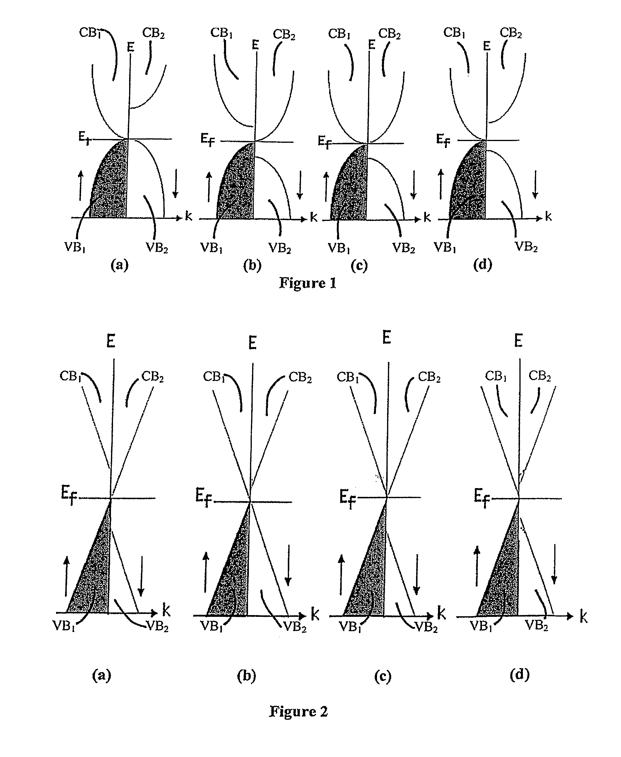
[0055]With reference to FIG. 1, specific examples of band structures of gapless semiconductor materials in accordance with the embodiments of present invention are now described.
[0056]FIG. 1 (a) shows a schematic representation of an energy band diagram of gapless semiconductor material in accordance with a first specific embodiment of the present invention. The shown band diagram illustrates a dispersion relation of the material (energy E as a function of momentum k). The energy band diagram shows the F...
PUM
| Property | Measurement | Unit |
|---|---|---|
| Energy | aaaaa | aaaaa |
| Energy | aaaaa | aaaaa |
| Energy | aaaaa | aaaaa |
Abstract
Description
Claims
Application Information