Solid-state imaging device, electronic apparatus, and method for making solid-state imaging device

a solid-state imaging and electronic equipment technology, applied in the direction of electrical equipment, semiconductor devices, radio frequency controlled devices, etc., can solve the problems of difficult to employ this process to form a photodiode, large amount of misalignment between the transfer gate electrode and the photodiode, and the inability to achieve the effect of forming a photodiode, so as to improve the image quality of captured images

Inactive Publication Date: 2011-02-24
SONY CORP
View PDF3 Cites 12 Cited by
  • Summary
  • Abstract
  • Description
  • Claims
  • Application Information

AI Technical Summary

Benefits of technology

[0008]When the photodiode does not extend under pixel transistors other than the transfer transistors, the transfer gate electrode can be formed first and then ions can be implanted in a self-aligning manner using the transfer electrode as a mask. This can eliminate misalignment between the photodiode and the pixel transistors other than the transfer transistor.
[0009]However, it is difficult to employ this process to form a photodiode that extends under a pixel transistor other than the transfer transistor. Thus, misalignment between the transfer transistor and the photodiode may still occur. As a result, the efficiency of transferring signal charges from the photodiode to a floating diffusion may decrease and the quality of images captured may degrade.
[0010]It is desirable to provide a solid-state imaging device and an electronic apparatus that can improve the image quality of captured images and a method for making the solid-state imaging device.
[0013]In this embodiment, the same mask is used to form the third region and remove the first region. Thus, the third region can be formed in a self-aligning manner. Then a transfer gate electrode is formed to extend from above the channel-forming region in the portion from which the first region is removed to above the photoelectric conversion unit. The transfer gate electrode is used as a mask to form a readout drain in a self-aligning manner. Thus, misalignment between the transfer gate electrode and the photoelectric conversion unit and between the transfer gate electrode and the readout drain does not occur. As a result, the decrease in efficiency of transferring signal charges caused by misalignment can be suppressed.
[0015]According to this embodiment, the positional relationship between the transfer gate electrode and the photoelectric conversion unit is determined by the step. Thus, there is no adverse effect of misalignment, and the efficiency of transferring signal charges improves.
[0017]According to the embodiments of the present invention, a solid-state imaging device and an electronic apparatus that can improve the image quality of captured images and a method for making the solid-state imaging device can be provided.

Problems solved by technology

However, this may cause a large amount of misalignment between the transfer gate electrode and the photodiode.
However, it is difficult to employ this process to form a photodiode that extends under a pixel transistor other than the transfer transistor.
Thus, misalignment between the transfer transistor and the photodiode may still occur.
As a result, the efficiency of transferring signal charges from the photodiode to a floating diffusion may decrease and the quality of images captured may degrade.

Method used


Image

  • Solid-state imaging device, electronic apparatus, and method for making solid-state imaging device
  • Solid-state imaging device, electronic apparatus, and method for making solid-state imaging device
  • Solid-state imaging device, electronic apparatus, and method for making solid-state imaging device

Examples


first embodiment

1. First Embodiment

[A] Device Configuration

(1) Overall Configuration of Camera

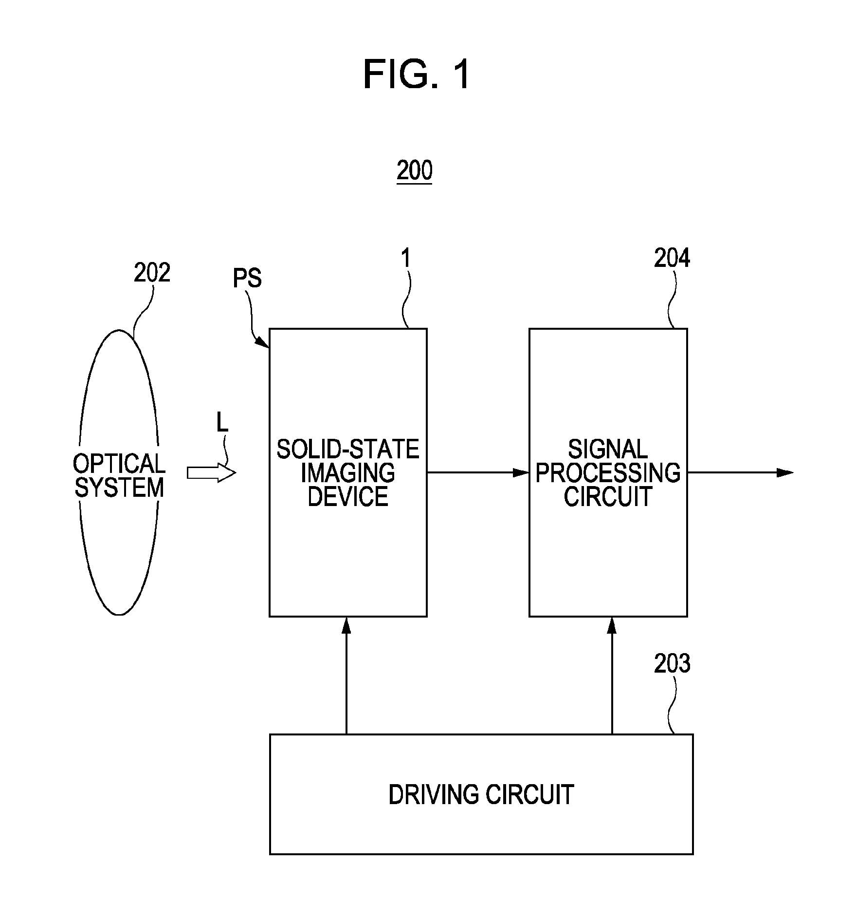
[0039]FIG. 1 is a diagram showing a configuration of a camera according to an embodiment of the present invention.

[0040]As shown in FIG. 1, a camera 200 includes a solid-state imaging device 1, an optical system 202, a driving circuit 203, and a signal processing circuit 204 which are described below.

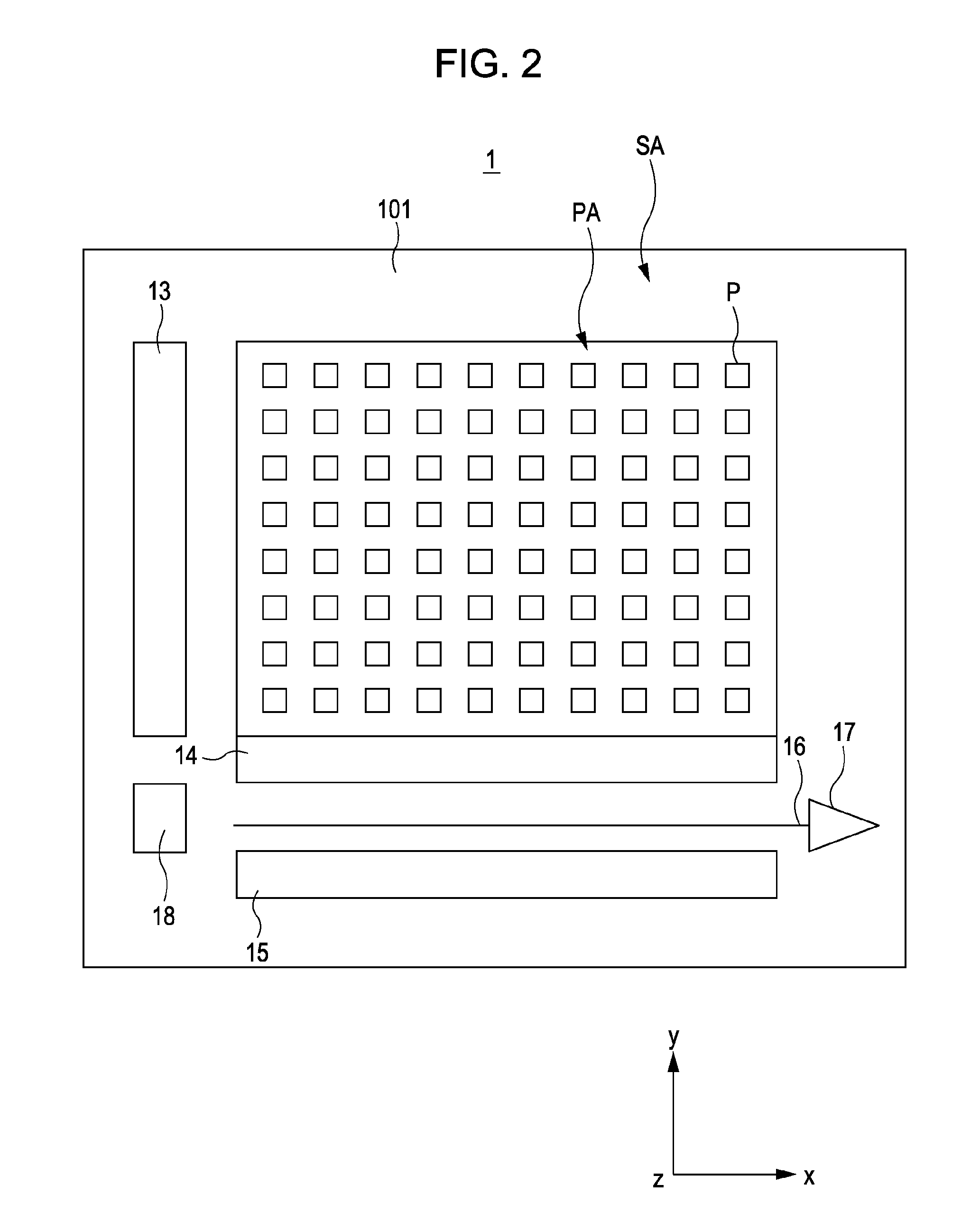
[0041]The solid-state imaging device 1 has a surface that receives incident light (image of an object to be captured) that has entered through the optical system 202. The solid-state imaging device 1 converts the incident light into electric charges to generate signal charges and outputs raw data. The solid-state imaging device 1 is driven in accordance with control signals output from the driving circuit 203. The detailed structure of the solid-state imaging device 1 is described below.

[0042]The optical system 202 includes an imaging lens (not shown) and a diaphragm (not shown) and is arranged so that the inc...

second embodiment

2. Second Embodiment

[A] Device Configuration

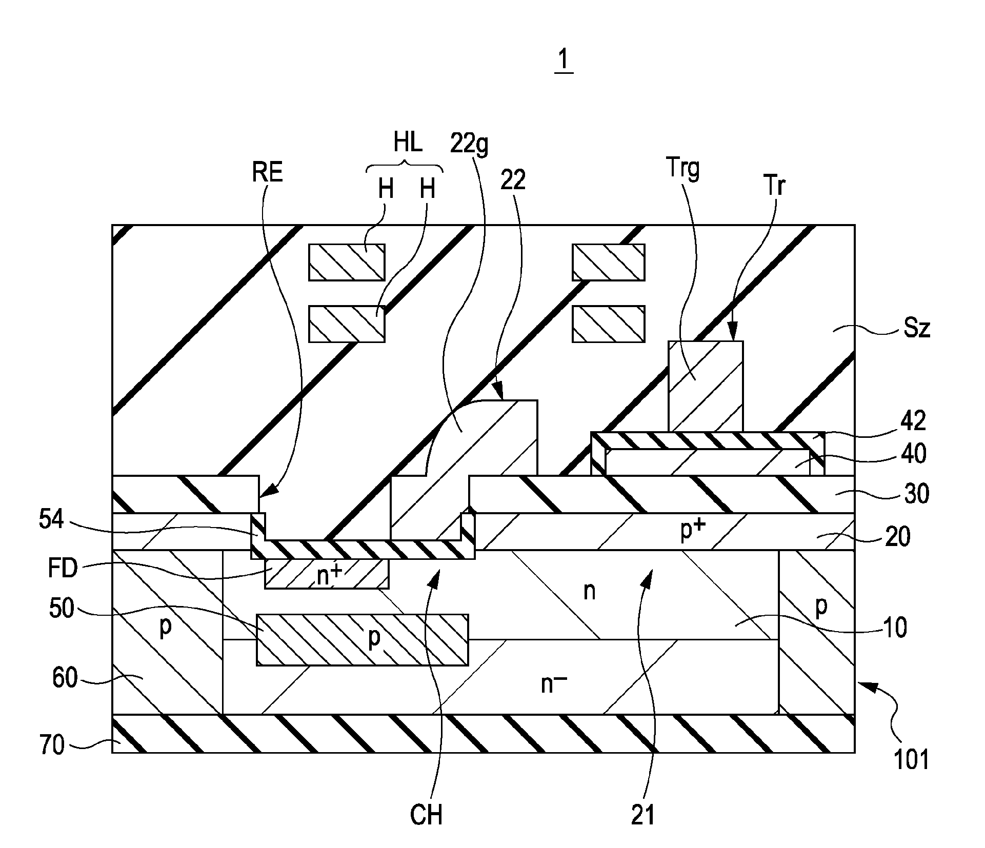
[0164]FIG. 10 is a cross-sectional view of a solid-state imaging device according to a second embodiment of the present invention.

[0165]As shown in FIG. 10, a solid-state imaging device 1b of this embodiment differs from the first embodiment in the arrangement of the transfer gate electrode (transfer gate electrode 22gb). The second embodiment is the same as the first embodiment in other features. Thus, the description is simplified to avoid redundancy.

[0166]As shown in FIG. 10, the transfer gate electrode 22gb is formed on a gate insulating film 54b and continuously extends from a part of a trench REb to the upper surface of a p-type semiconductor layer 20b of a photodiode 21b. In other words, the transfer gate electrode 22gb continuously extends from above a channel-forming region CHb to above the p-type semiconductor layer 20b with the gate insulating film 54b therebetween. The solid-state imaging device 1b has the same configuration as...

third embodiment

3. Third Embodiment

[A] Device Configuration

[0181]FIG. 12 is a cross-sectional view of a solid-state imaging device according to a third embodiment of the present invention.

[0182]As shown in FIG. 12, a solid-state imaging device 1c of this embodiment differs from the first embodiment in the arrangement of the transfer gate electrode (transfer gate electrode 22gc). The third embodiment is the same as the first embodiment in other features. Thus, the description is simplified to avoid redundancy.

[0183]As shown in FIG. 12, the transfer gate electrode 22gc continuously extends from a part of a gate insulating film 54c above a channel-forming region CHc to a part of a gate insulating film 42c on a silicon film 40c above a photodiode 21c. The solid-state imaging device 1c has the same configuration as the first embodiment except for this.

[0184]In this embodiment, the transfer gate electrode 22gc is formed not on the a buried oxide film 30c but on the gate insulating film 42c. The size of t...


PUM


Abstract

A solid-state imaging device includes a photoelectric conversion unit that includes a first region of a first conductivity type and a second region of a second conductivity type between which a pn junction is formed, the first region and the second region being formed in a signal-readout surface of a semiconductor substrate, the second region being located at a position deeper than the first region; and a transfer transistor configured to transfer signal charges accumulated in the photoelectric conversion unit to a readout drain through a channel region that lies under a surface of the first region and horizontally adjacent to the photoelectric conversion unit, the transfer transistor being formed in the signal-readout surface. The transfer transistor includes a transfer gate electrode that extends from above the channel region with a gate insulating film therebetween to above the first region so as to extend across a step.

Description

BACKGROUND OF THE INVENTION[0001]1. Field of the Invention[0002]The present invention relates to a solid-state imaging device, an electronic apparatus, and a method for making a solid-state imaging device.[0003]2. Description of the Related Art[0004]Electronic apparatuses such as digital video cameras and digital still cameras include solid-state imaging devices. Examples of the solid-state imaging devices included in electronic apparatuses include complementary metal oxide semiconductor (CMOS)-type image sensors and charge coupled device (CCD)-type image sensors.[0005]A solid-state imaging device has an imaging region on a surface of a semiconductor substrate. The imaging region is where a plurality of pixels are formed. A plurality of photoelectric conversion elements corresponding to the pixels are also formed in the imaging region. Photoelectric conversion elements receive light from an object to be captured and convert the light into electric charges to generate signal charges....

Claims


Application Information

Patent Timeline
Patent Type & Authority Applications(United States)
IPC IPC(8): H01L31/08H01L31/18H01L31/14
CPCH01L27/14609H01L27/14689H01L27/14641H01L27/14612H01L27/14692
Inventor MABUCHI, KEIJI
Owner SONY CORP
Why Eureka
Try Eureka