Enhanced solderability using a substantially pure nickel layer deposited by physical vapor deposition

a nickel layer and physical vapor deposition technology, applied in the direction of liquid/solution decomposition chemical coating, superimposed coating process, soldering apparatus, etc., can solve the problems of preventing reliable solder connection and reliability problems, and achieve reliable solder connection, eliminate solderability and reliability problems, good adhesion

Inactive Publication Date: 2011-03-03
ARMY US SEC THE
View PDF9 Cites 5 Cited by
  • Summary
  • Abstract
  • Description
  • Claims
  • Application Information

AI Technical Summary

Benefits of technology

[0004]A preferred embodiment of the present invention is a method to provide reliable solder connections to nickel plated electronics boards and parts, including quick turnaround prototype circuits and device evaluation circuits. This method relies on a high purity nickel layer deposited by a suitable physical vapor deposition (PVD) technique, such as e-beam evaporation, sputtering, etc., on an existing nickel plated nickel layer. The high purity layer (i.e. approximately at least 99.98% purity) eliminates solderability and reliability problems often associated with soldering directly to plated nickel films. The basic process steps flow for this method comprise: (1) preparing a substrate for nickel plating; (2) plating the nickel film to desired thickness using desired plating method; (3) preparing the nickel film for evaporation by thoroughly cleaning the film—the surface; may also be slightly roughened to insure good adhesion to deposited nickel film; and (4) depositing the substantially pure nickel film using a suitable PVD technique.

Problems solved by technology

However, the contamination in the nickel from the plating processes can prevent reliable solder connections from being made.
Although some nickel plating processes, such as a low phosphorus process, can improve the solderability conditions, problems with reliability can still occur with high currents over a long period of time due to the contamination species in the nickel films.

Method used


Image

  • Enhanced solderability using a substantially pure nickel layer deposited by physical vapor deposition

Examples


Embodiment Construction

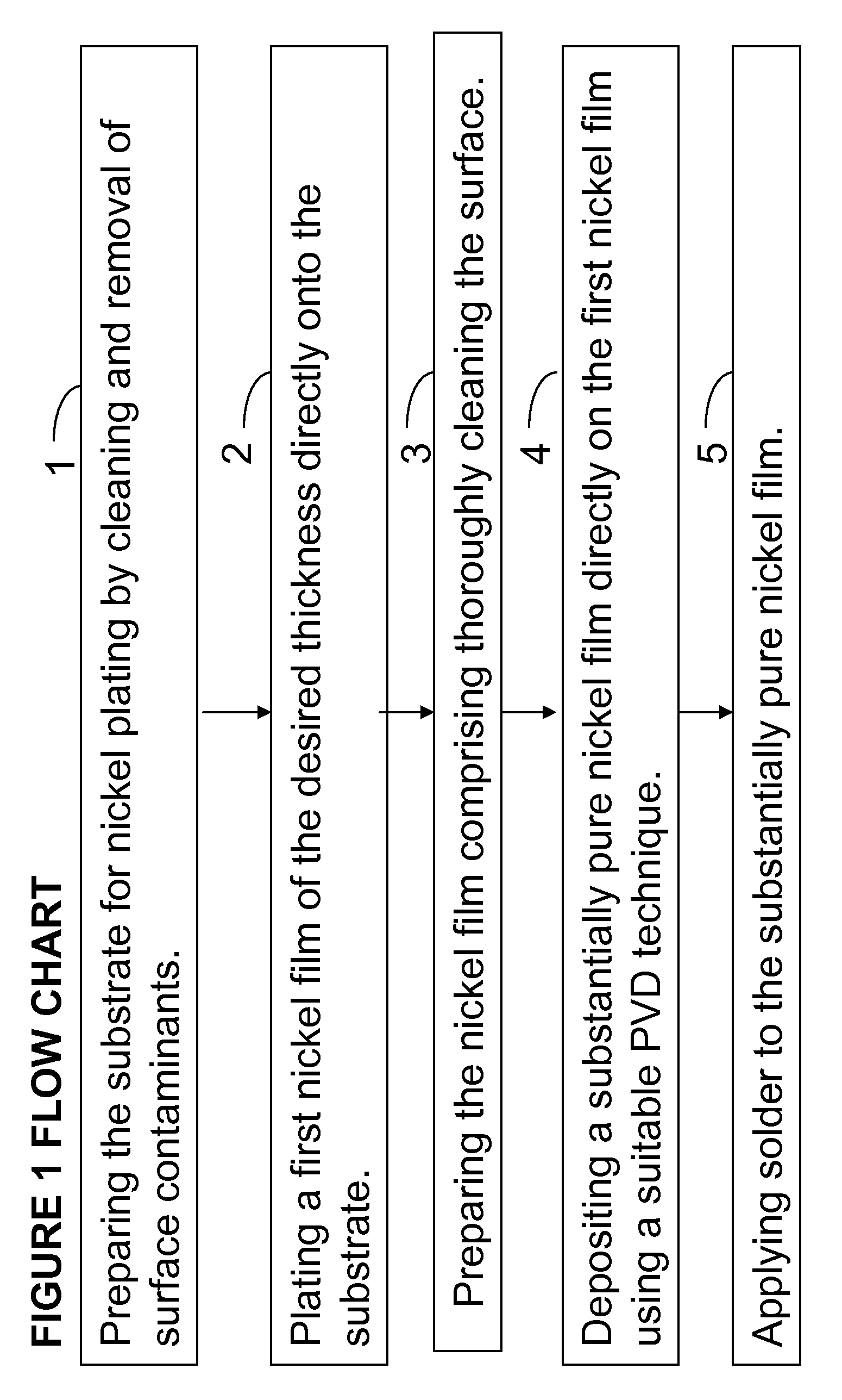
[0007]The present invention now will be described more fully hereinafter with reference to the accompanying drawings, in which embodiments of the invention are shown. However, this invention should not be construed as limited to the embodiments set forth herein. Rather, these embodiments are provided so that this disclosure will be thorough and complete, and will fully convey the scope of the invention to those skilled in the art.

[0008]The terminology used herein is for the purpose of describing particular embodiments only and is not intended to limit the full scope of the invention. As used herein, the singular forms “a”, “an” and “the” are intended to include the plural forms as well, unless the context clearly indicates otherwise. It will be further understood that the terms “comprises” and / or “comprising,” when used in this specification, specify the presence of stated features, integers, steps, operations, elements, and / or components, but do not preclude the presence or additio...


PUM

PropertyMeasurementUnit
thicknessaaaaaaaaaa
thicknessaaaaaaaaaa
purityaaaaaaaaaa

Abstract

A first preferred method for increasing the solderability of a substrate comprising: preparing the substrate for nickel plating by cleaning and removal of surface contaminants; plating a first nickel film of the desired thickness directly onto the substrate; preparing the nickel film comprising thoroughly cleaning the surface; depositing a substantially pure nickel film directly on the first nickel film using a suitable PVD technique; and applying solder to the substantially pure nickel film. Another preferred method for increasing the solderability of a substrate comprising plating a first nickel layer directly onto the substrate by using an electrolytic or electroless nickel plating process; depositing a substantially pure nickel film directly on the first nickel film using physical vapor deposition; and applying solder to the substantially pure nickel film.

Description

GOVERNMENT INTEREST[0001]The invention described herein may be manufactured, used, and / or licensed by or for the United States Government.FIELD OF THE INVENTION[0002]This invention relates generally to soldering, and more particularly to coatings which increase the solderability or effectiveness of a solder joint.BACKGROUND OF THE INVENTION[0003]Current practice is to solder directly to the nickel plate used in electronics assemblies. However, the contamination in the nickel from the plating processes can prevent reliable solder connections from being made. Although some nickel plating processes, such as a low phosphorus process, can improve the solderability conditions, problems with reliability can still occur with high currents over a long period of time due to the contamination species in the nickel films. Other nickel soldering processes rely on more complicated techniques such as inter-layers and reflow operations to improve the solder to nickel bond. See for example Y. M. Cho...

Claims


Application Information

Patent Timeline
Patent Type & Authority Applications(United States)
IPC IPC(8): C23C14/34C25D5/02
CPCB23K1/0016B23K1/20B23K2201/40C25D5/48C23C14/16C23C18/165C23C18/32C23C14/025B23K2101/40
Inventor ROD, BERNARD J.
Owner ARMY US SEC THE
Why Eureka
Try Eureka