Handshake structure for improving layout density

Active Publication Date: 2011-03-03
ADVANCED MICRO DEVICES INC
View PDF5 Cites 15 Cited by
  • Summary
  • Abstract
  • Description
  • Claims
  • Application Information

AI Technical Summary

Benefits of technology

[0016]In certain embodiments, an integrated circuit includes one or more semiconductor devices. At least one of the semiconductor devices includes the gate with one side wall of the gate including at least one protrusion and an opposite side wall of the gate including at least one depression, the insulating layer disposed substantially over the gate, the contact formed through the insulating layer, and the metal layer with the first structure disposed on the insulating layer.
[0017]In certain embodiments, a computer readable storage medium stores a plurality of instructions which, when executed, generate one or more patterns useable to provide a semiconductor device that includes the gate with one side wall of the gate including at least one protrusion and an opposite side wall of the g

Problems solved by technology

A first challenge in routing M1 wires (either contact wires or vertical wires) is misalignment, or overlay error.
Misalignment is an increasing challenge in modern lithography, which results in certain practical limitations.
One practical limitation is that the offset between small contacting features is desired to be kept as small as possible with coinciding centers being preferred.
A second challenge is the desire for CPP (contacted poly pitch) to be close to limits of technology (for example, 22 nm design rules).
This method, however, increases the overall chip area and limits the performance of the chip versus chip area.
The additional V0 layer may significantly increase development and/or processing costs.
This makes it difficult to route wires from other locations (for example, other logic gates or othe

Method used


Image

  • Handshake structure for improving layout density
  • Handshake structure for improving layout density
  • Handshake structure for improving layout density

Examples


Embodiment Construction

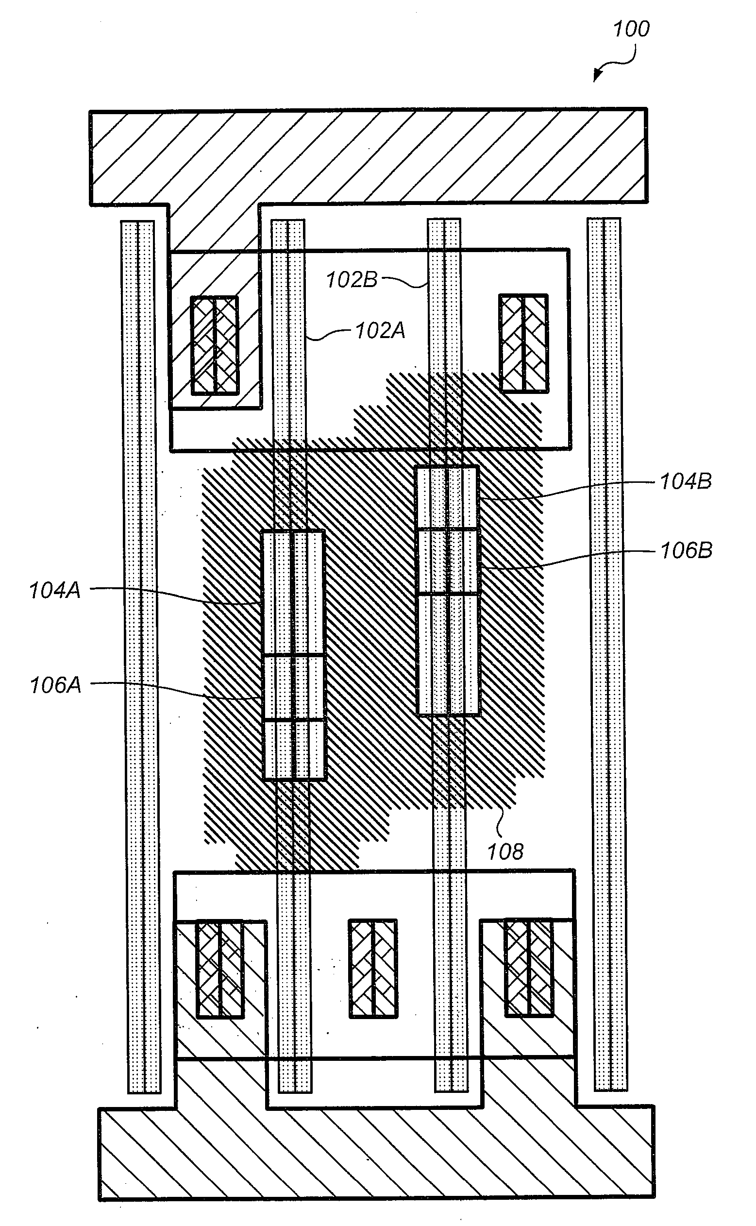
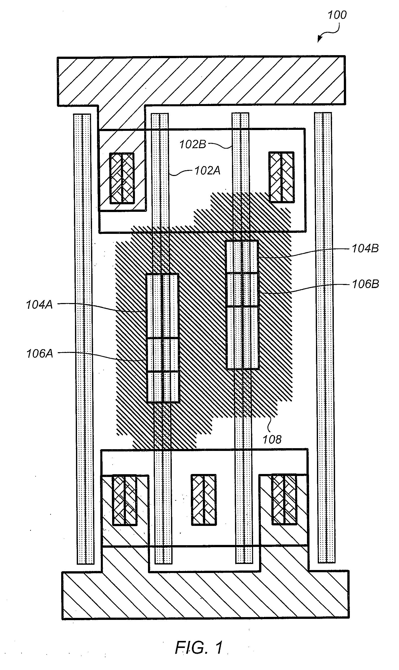
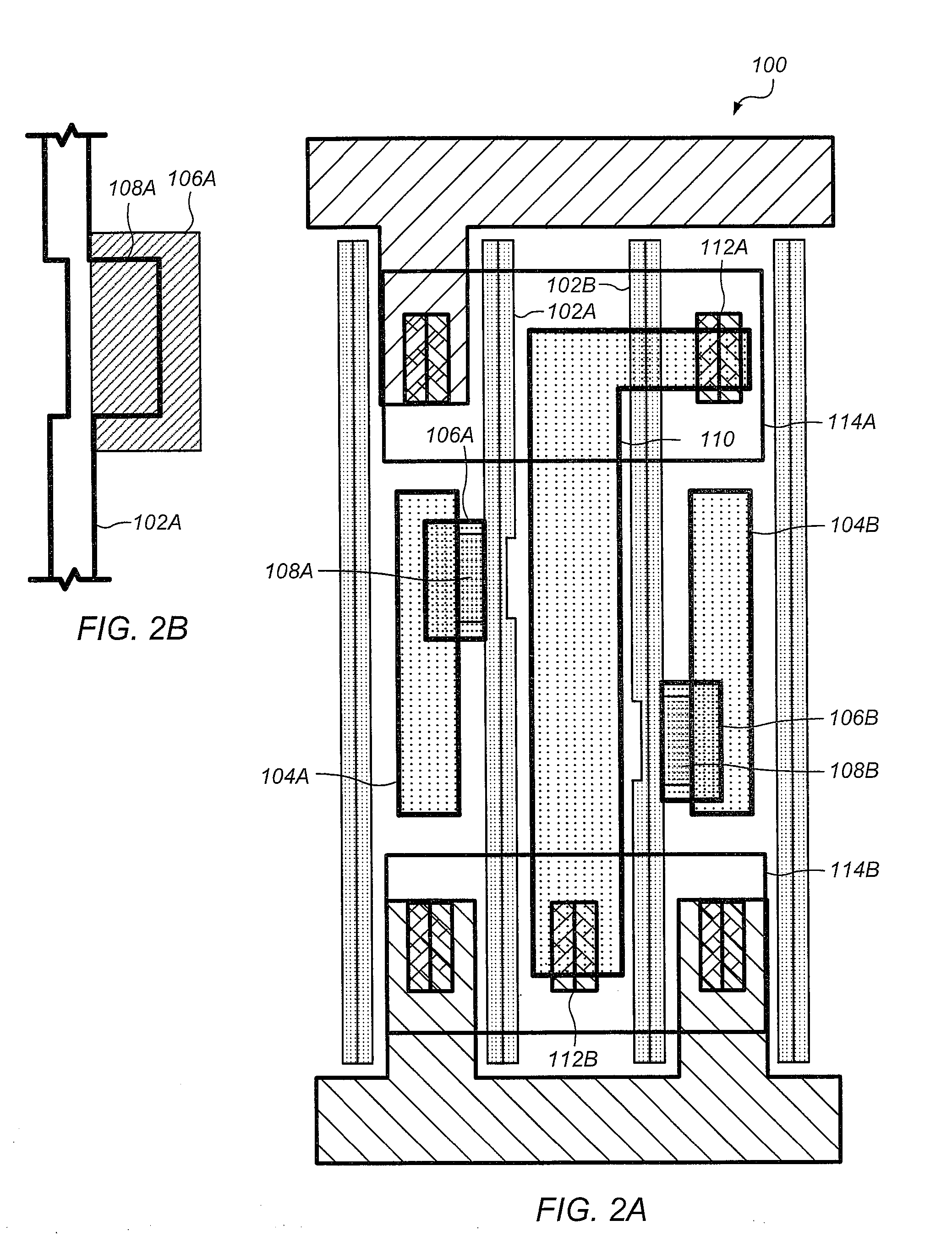
[0014]In certain embodiments, a semiconductor device includes a gate on a semiconductor substrate. One side wall of the gate may include at least one protrusion and an opposite side wall of the gate may include at least one depression. An insulating layer may be disposed substantially over the gate. A contact may be formed through the insulating layer. The contact may at least partially overlap at least one of the protrusions in the gate. A metal layer may be disposed on the insulating layer. The metal layer may include a first metal layer structure shifted to a first side of the gate. The first structure may at least partially overlap the contact such that the contact electrically couples the first structure to the gate through the insulating layer.

[0015]In certain embodiments, a semiconductor device fabrication process includes forming the gate on the semiconductor substrate with one side wall of the gate including at least one protrusion and an opposite side wall of the gate incl...


PUM


Abstract

A semiconductor device includes a gate on a semiconductor substrate. One side wall of the gate may include at least one protrusion and an opposite side wall of the gate may include at least one depression. A contact is formed through an insulating layer disposed over the gate. The contact at least partially overlaps at least one of the protrusions in the gate. A metal layer is disposed on the insulating layer. The metal layer includes a first structure shifted to a first side of the gate. The first structure at least partially overlaps the contact such that the contact electrically couples the first structure to the gate through the insulating layer.

Description

BACKGROUND OF THE INVENTION[0001]1. Field of the Invention[0002]This invention relates generally to semiconductor processes for forming transistors and, more specifically, to processes for increasing layout density on a semiconductor substrate.[0003]2. Description of the Related Art[0004]Transistors such as planar transistors have been the core of integrated circuits for several decades. During the use of transistors, the size of the individual transistors has steadily decreased through advances in process development and the need to increase feature density. Current scaling employs 32 nm technologies with development progressing towards 22 nm technologies.[0005]Metal 1 (M1) vertical wire routes used to connect between NMOS and PMOS structures are important in standard transistor cell designs. The M1 vertical wire routes may connect to contacts (outputs) that contact to active areas of the underlying layer. The M1 vertical wire routes may be in addition to other M1 wires that contac...

Claims


Application Information

Patent Timeline
IPC IPC(8): H01L27/088H01L21/28
CPCH01L21/76895H01L21/823456H01L21/823475H01L23/485H01L27/0207H01L2924/0002H01L27/088H01L29/4238H01L2924/00H01L29/423H01L21/8234
Inventor CARLSON, ANDREW E.
Owner ADVANCED MICRO DEVICES INC
Why Eureka
Try Eureka