Semiconductor device and method for manufacturing the same

a technology of semiconductors and semiconductors, applied in the direction of semiconductor devices, basic electric elements, electrical appliances, etc., can solve the problems of difficult control of circuits including thin film transistors, inability to perform switching functions, and malfunctions, etc., to achieve stable electric characteristics, favorable electric characteristics, and high reliability

Inactive Publication Date: 2011-03-17
SEMICON ENERGY LAB CO LTD
View PDF117 Cites 50 Cited by
  • Summary
  • Abstract
  • Description
  • Claims
  • Application Information

AI Technical Summary

Benefits of technology

[0017]A thin film transistor whose threshold voltage does not change greatly and whose electric characteristics are stable can be manufactured. T

Problems solved by technology

When the threshold voltage of the thin film transistor is high or negative even when the field effect mobility is high, it is difficult to control a circuit including the thin film transistor.
When the thin film transistor has a high threshold voltage and a large absolute value of its threshold voltage, the thin film transistor cannot perform a switching function as a TFT when the thin film transistor is driven at low voltage and may be a load.
A thin film transistor i

Method used


Image

  • Semiconductor device and method for manufacturing the same
  • Semiconductor device and method for manufacturing the same
  • Semiconductor device and method for manufacturing the same

Examples


embodiment 1

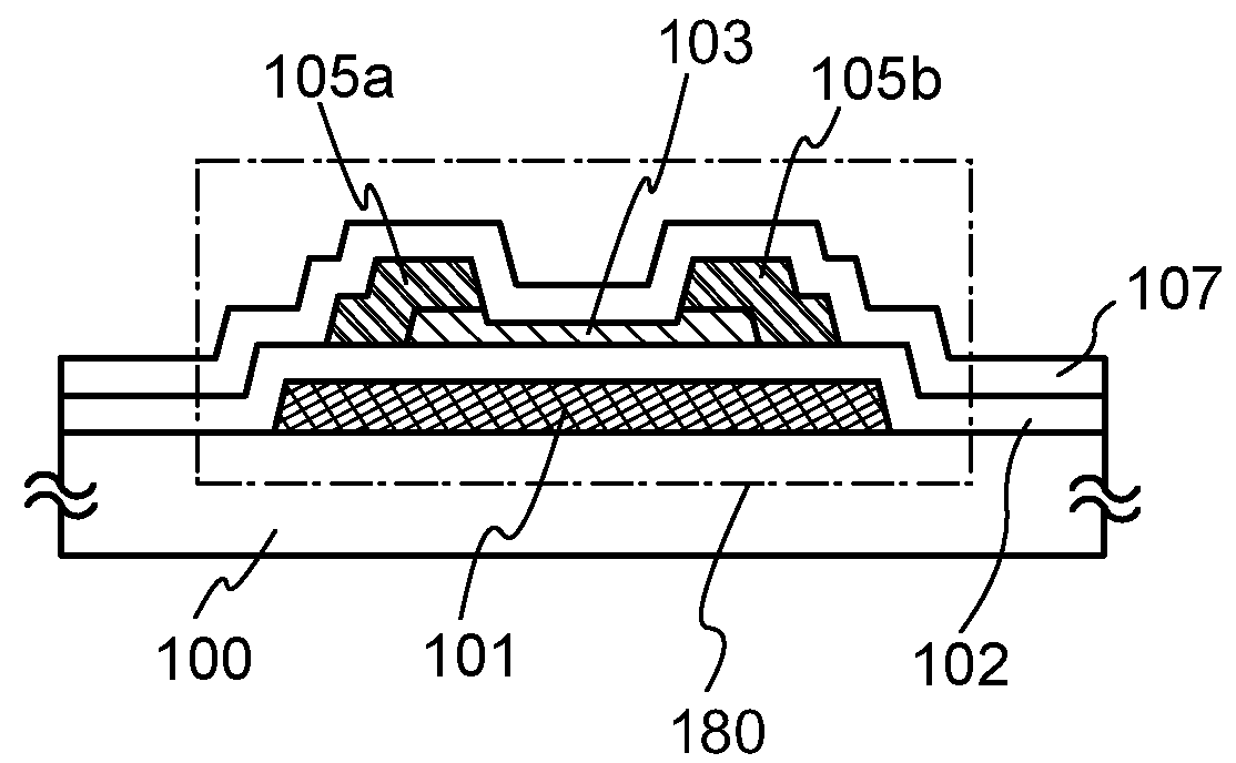
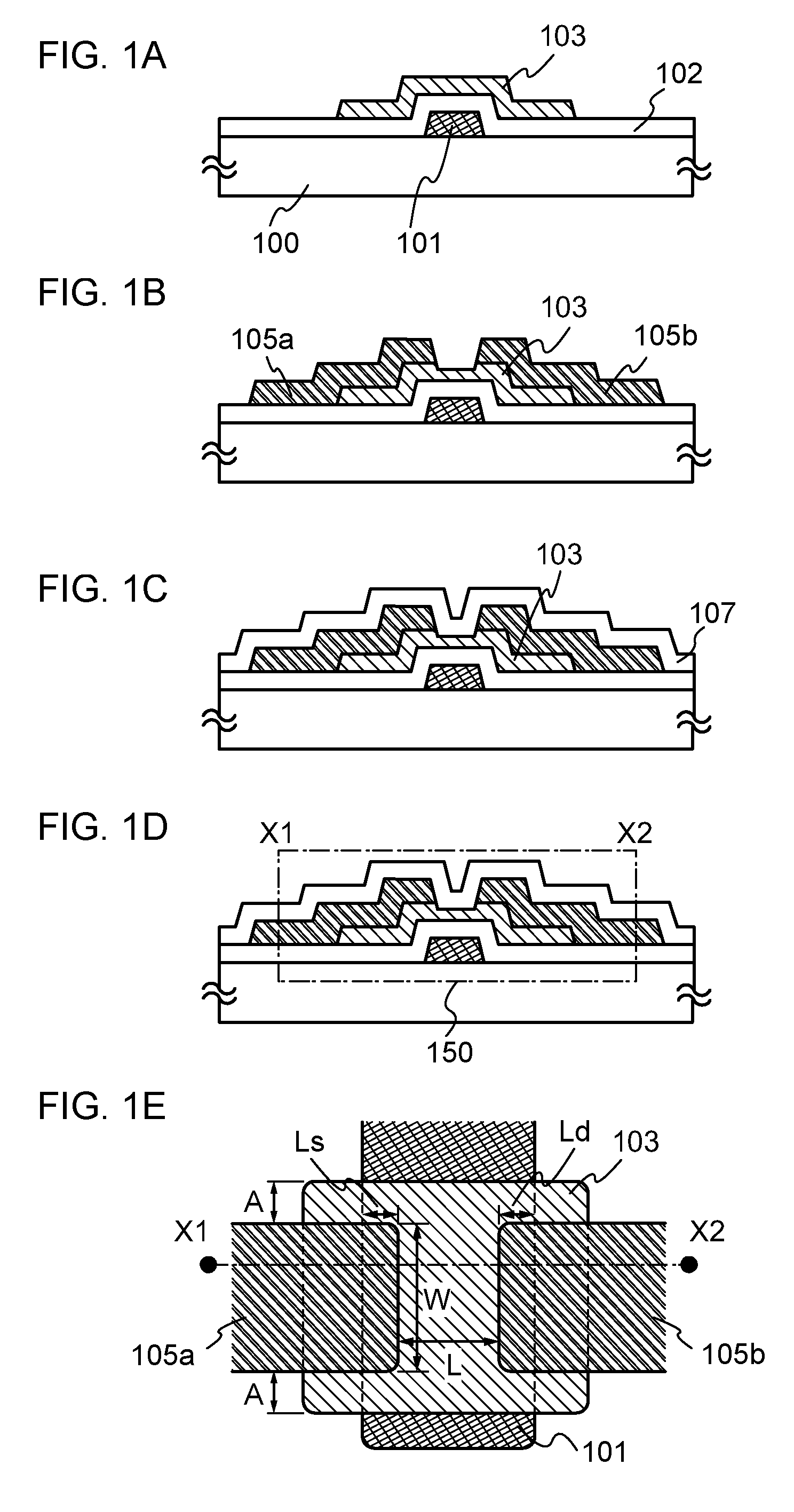
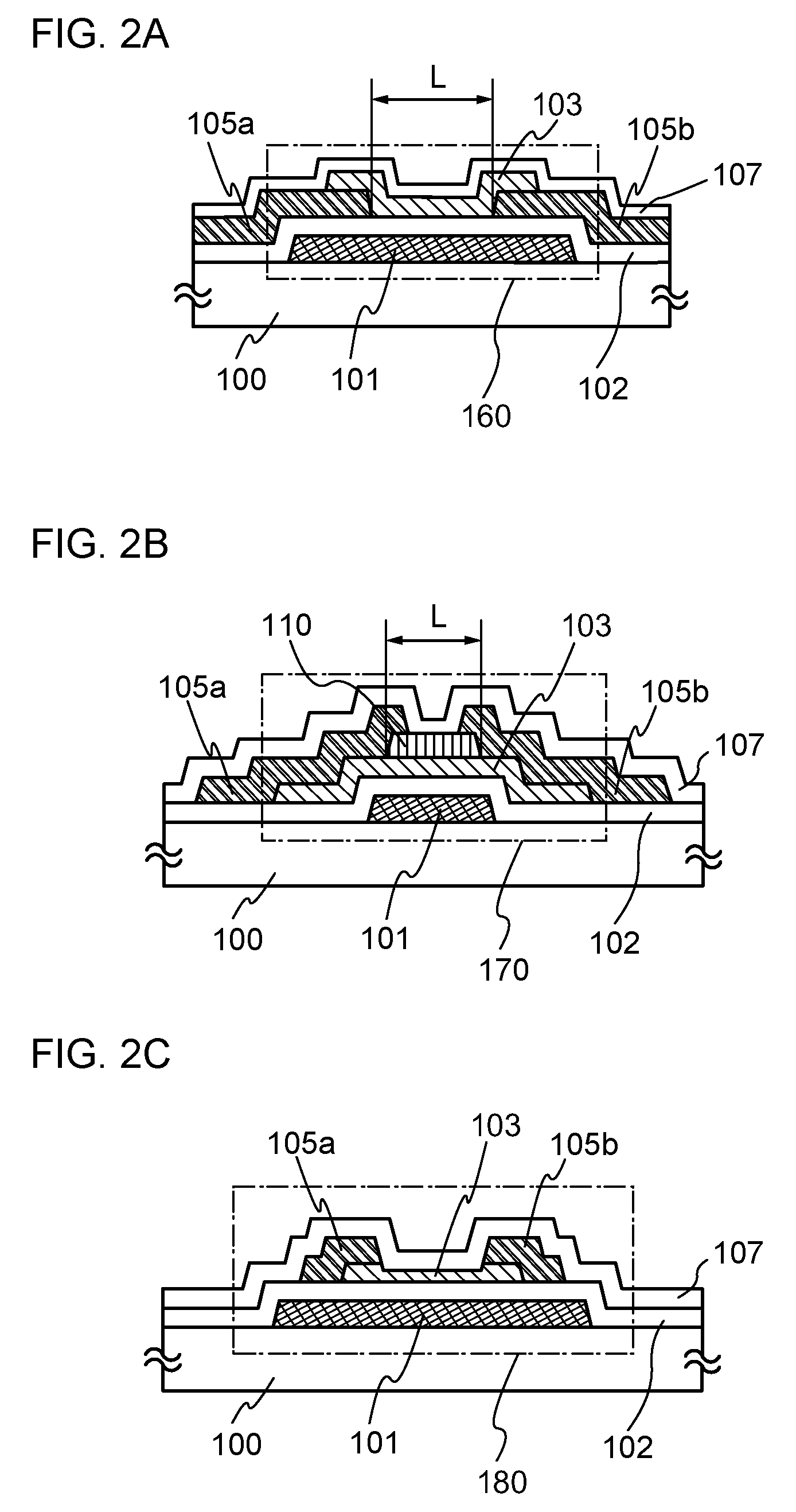
[0056]In this embodiment, an embodiment of a method for manufacturing a thin film transistor 150 illustrated in FIG. 1D will be described with reference to FIGS. 1A to 1D which are cross-sectional views illustrating a manufacturing process of a thin film transistor. FIG. 1E is a top view of the thin film transistor 150 illustrated in FIG. 1D. The thin film transistor 150 is a kind of bottom-gate transistor called a channel-etched transistor and also a kind of an inverted staggered transistor.

[0057]First, over a substrate 100 which is a substrate having an insulating surface, a gate electrode layer 101 is provided through a photolithography step with the use of a photomask. Note that a resist mask may be formed by an ink-jet method. When the resist mask is formed by an ink-jet method, manufacturing costs can be reduced because a photomask is not used.

[0058]It is preferable that a glass substrate be used as the substrate 100. When the temperature of heat treatment performed later is h...

embodiment 2

[0133]In this embodiment, an example will be described below in which at least part of a driver circuit and a thin film transistor arranged in a pixel portion are formed over one substrate.

[0134]The thin film transistor arranged in the pixel portion is formed in accordance with Embodiment 1. The thin film transistor described in Embodiment 1 is an n-channel TFT, and thus, part of a driver circuit that can include an n-channel TFT among driver circuits is formed over the same substrate as the thin film transistor of the pixel portion.

[0135]FIG. 7A illustrates an example of a block diagram of an active matrix display device. Over a substrate 5300 in the display device, a pixel portion 5301, a first scan line driver circuit 5302, a second scan line driver circuit 5303, and a signal line driver circuit 5304 are provided. In the pixel portion 5301, a plurality of signal lines extended from the signal line driver circuit 5304 are arranged and a plurality of scan lines extended from the fi...

embodiment 3

[0175]In this embodiment, the case where thin film transistors are manufactured and a semiconductor device (also referred to as a display device) having a display function in which the thin film transistors are used for a pixel portion and a driver circuit is manufactured will be described. Further, part or whole of the driver circuit can be formed over the same substrate as the pixel portion with the use of a thin film transistor, whereby a system-on-panel can be obtained.

[0176]The display device includes a display element. As the display element, a liquid crystal element (also referred to as a liquid crystal display element) or a light-emitting element (also referred to as a light-emitting display element) can be used. The light-emitting element includes, in its category, an element whose luminance is controlled by a current or a voltage, and specifically includes, in its category, an inorganic electroluminescent (EL) element, an organic EL element, and the like. Furthermore, a di...


PUM


Abstract

It is an object to provide a highly reliable thin film transistor with stable electric characteristics, which includes an oxide semiconductor film. The channel length of the thin film transistor including the oxide semiconductor film is in the range of 1.5 μm to 100 μm inclusive, preferably 3 μm to 10 μm inclusive; when the amount of change in threshold voltage is less than or equal to 3 V, preferably less than or equal to 1.5 V in an operation temperature range of room temperature to 180° C. inclusive or −25° C. to −150° C. inclusive, a semiconductor device with stable electric characteristics can be manufactured. In particular, in a display device which is an embodiment of the semiconductor device, display unevenness due to variation in threshold voltage can be reduced.

Description

TECHNICAL FIELD[0001]The present invention relates to a semiconductor device including an oxide semiconductor and a manufacturing method thereof.[0002]In this specification, a semiconductor device generally means a device which can function by utilizing semiconductor characteristics, and an electro-optical device, a semiconductor circuit, and an electronic device are all semiconductor devices.BACKGROUND ART[0003]In recent years, a technique for forming a thin film transistor (TFT) by using a semiconductor thin film (having a thickness of approximately several nanometers to several hundred nanometers) formed over a substrate having an insulating surface has attracted attention. Thin film transistors are applied to a wide range of electronic devices such as ICs or electro-optical devices, and prompt development of thin film transistors that are to be used as switching elements in image display devices, in particular, is being pushed. Various metal oxides are used for a variety of appl...

Claims


Application Information

Patent Timeline
IPC IPC(8): H01L29/12H01L21/16
CPCH01L29/7869H01L29/66969H01L29/78696H01L29/66742H01L29/78606
Inventor YAMAZAKI, SHUNPEITSUBUKU, MASASHIGODO, HIROMICHI
Owner SEMICON ENERGY LAB CO LTD
Why Eureka
Try Eureka