Semiconductor device and data processing system comprising semiconductor device

a semiconductor device and data processing technology, applied in the field of semiconductor devices, can solve the problems of increasing the operation current required in pre-charge operations or the like, and achieve the effect of reducing the operation current and reducing the operating curren

Inactive Publication Date: 2011-03-17
PS4 LUXCO SARL
View PDF4 Cites 11 Cited by
  • Summary
  • Abstract
  • Description
  • Claims
  • Application Information

AI Technical Summary

Benefits of technology

[0012]As describe above, according to the present invention, when the signal from the sense amplifier circuit to the read amplifier circuit through hierarchical data lines, the gate voltage applied to transistors included in the second / third switch circuits can be relatively small, and thus the operating current required for a precharge operation or the like can be reduced. Particularly, in a case where the parasitic capacitance increases due to a long main data line, or a case where the number of output bits to be read simultaneously is increased, the effect of reducing the operation current in the present invention can be drastic. Further, high-speed sensing can be achieved for the signal with a small amplitude which is half the small amplitude in the conventional configuration.

Problems solved by technology

Therefore, the voltage difference of the main data lines having a large parasitic capacitance is required to have a sufficiently large amplitude in order that an amplitude at the final stage amplifier becomes sufficiently large, and there is a problem that an operation current required in a precharge operation or the like increases.

Method used


Image

  • Semiconductor device and data processing system comprising semiconductor device
  • Semiconductor device and data processing system comprising semiconductor device
  • Semiconductor device and data processing system comprising semiconductor device

Examples


first embodiment

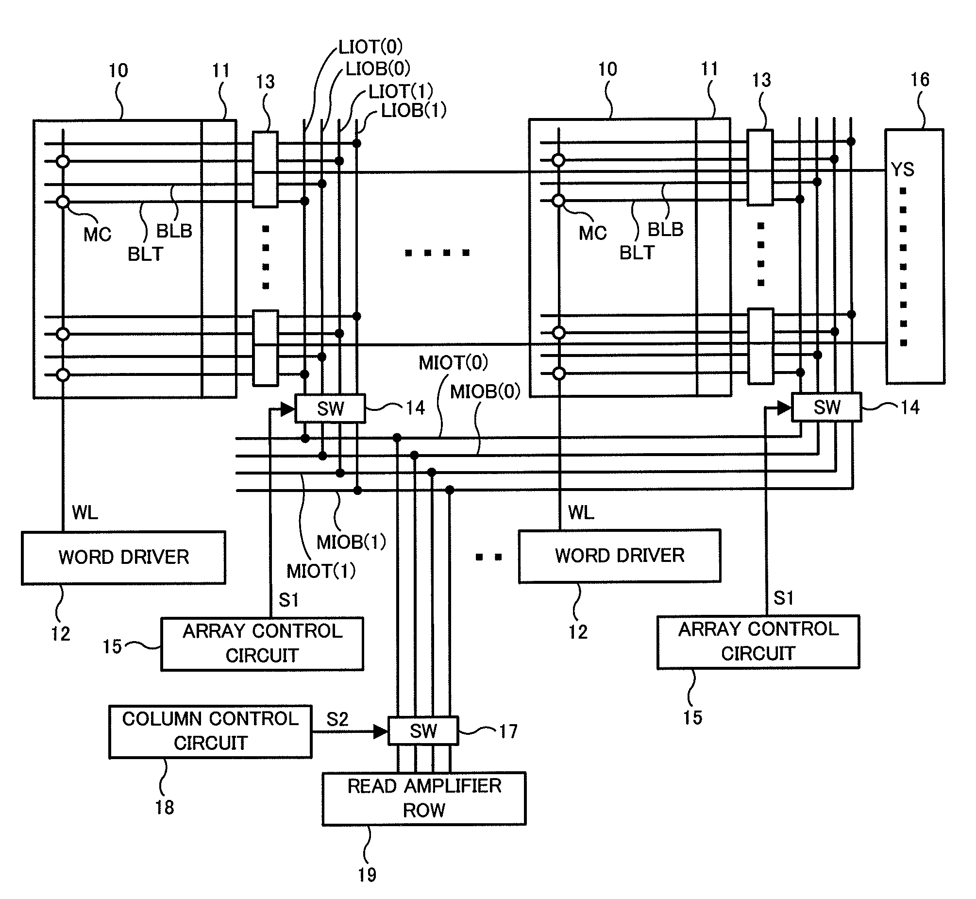
[0027]The first embodiment of the present invention will be described below. FIG. 1 is a block diagram mainly showing an entire configuration of column circuits in a DRAM of the first embodiment. In the block diagram of FIG. 1, a plurality of memory cell arrays 10 are provided, and a sense amplifier row 11, a word driver 12, a predetermined number of column select circuits 13, a switch circuit 14 and an array control circuit 15 are provided attached to each of the memory cell arrays 10. Further, a column decoder 16, a switch circuit 17, a column control circuit 18 and a read amplifier row 19 are provided attached to the entire column circuits. The plurality of memory cell arrays 10 are arranged in a bit line direction together with the sense amplifier rows 11 in the layout of the DRAM.

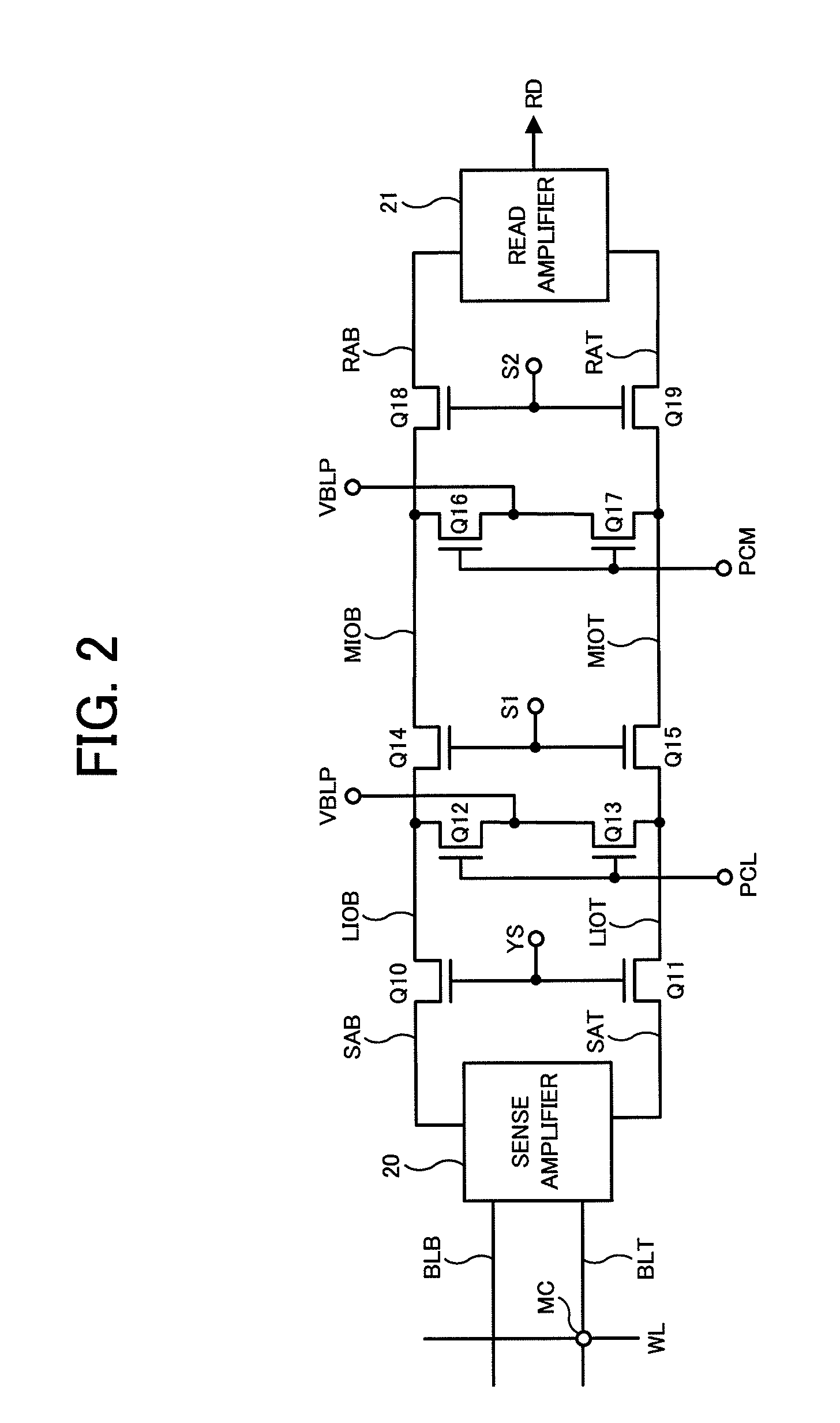
[0028]In each of the memory cell arrays 10, a plurality of word lines WL and a plurality of bit lines BLT / BLB intersecting the word lines WL are arranged, and a plurality of memory cells MC are formed ...

second embodiment

[0048]The second embodiment of the present invention will be described below. In the second embodiment, there is not provided a complementary configuration (T / B) using the pair of local data lines LIOT / LIOB and the pair of main data lines MIOT / MIOB as in the first embodiment. In contrast, the second embodiment employs a single-ended configuration using one local data line LIO and one main data line MIO, and has a feature that an amplifier 22 is arranged between the main data line MIO and the read amplifier 21a. In addition, components of the block diagram of FIG. 1 are common in the second embodiment if circuit portions corresponding to the bit line BL, the local data line LIO and the main data line MIO are replaced with single ended circuit configurations, so description thereof will be omitted.

[0049]FIG. 4 shows a specific circuit configuration of a portion of the read circuit in the DRAM of the second embodiment. The circuit configuration of FIG. 4 corresponds to the same range i...


PUM


Abstract

A semiconductor device comprises a sense amplifier circuit amplifying a signal transmitted through the bit line, first/second data lines transmitting the signal amplified by the sense amplifier circuit, a read amplifier circuit driven by a first voltage and amplifying the signal; first/second switch circuits controlling connection between the above components, first/second voltage setting circuits setting the second/third data lines to a second voltage lower than the first voltage. A predetermined voltage obtained by adding the second voltage to a threshold voltage of a transistor in the second/third switch circuit is applied to the gate terminal thereof, and ends of the data lines are connected to the source and drain terminals thereof.

Description

BACKGROUND OF THE INVENTION[0001]1. Field of the Invention[0002]The present invention relates to a semiconductor device having a configuration in which a signal read out from a memory cell and transmitted through a bit line is amplified by a sense amplifier.[0003]2. Description of Related Art[0004]Conventionally, a configuration of a semiconductor memory device such as a DRAM is known in which a sense amplifier sensing and amplifying a signal read out from a memory cell through a bit line and a read circuit transmitting an output signal of the sense amplifier to a final stage amplifier through hierarchical data lines (Refer to, for example, Japanese Patent Application Laid-open No. 2001-57080). In the above conventional read circuit, the output signal of the sense amplifier is transmitted sequentially from a local data line to a main data line and inputted to the final stage amplifier. Generally, an N-channel type transistor as a transfer gate is used to connect between the local da...

Claims


Application Information

Patent Timeline
Patent Type & Authority Applications(United States)
IPC IPC(8): G11C7/06
CPCG11C7/1048G11C7/1051G11C7/1069G11C2207/002G11C11/4096G11C11/4097G11C11/4091
Inventor YOSHIDA, SOICHIROKAJIGAYA, KAZUHIKOYAMADA, YASUTOSHI
Owner PS4 LUXCO SARL
Why Eureka
Try Eureka