Method for manufacturing semiconductor device or apparatus, and apparatus for manufacturing the same

Inactive Publication Date: 2011-03-17
CANON KK
View PDF2 Cites 60 Cited by
  • Summary
  • Abstract
  • Description
  • Claims
  • Application Information

AI Technical Summary

Benefits of technology

[0046]The wavelength and intensity of light are different depending on the semiconductor device or apparatus, so that the values of the wavelength and intensity of light are the same as values when the semiconductor device or apparatus is actually used.
[0047]Also, the irradiation time of the predetermined light for irradiation is not particularly limited as long as the irradiation time is in a range that the effect of the present invention (threshold compensation effect) is obtained. However, if the irradiation time is too short, the effect of the present invention is not obtained, and if the irradiation time is too long, the effect is saturated even with irradiation for certain time or more, and the tact time during manufacture is long. Therefore, considering these, optimal time can be appropriately set. According to the knowledge of the inventors, the number of photons of light having an intensity of 1 mW/cm2 and a wavelength of 350 nm is 1.76×10¹⁵ for 1 second. When the intensity doubles, the number of photons doubles. When the wavelength doubles, the number of photons doubles. For example, when the band gap of a semiconductor film is 350 nm or less, and the number of traps is 1.76×10¹⁵/cm2, all traps are filled when the semiconductor film is irradiated with the light for 1 second. The number of traps of the semiconductor film used in the present invention is estimated to be 1×10¹⁵/cm2 or less, therefore, it is considered that when the semiconductor film is irradiated with the light for 1 second or more, the effect of the present invention is obtained. In the present invention, irradiation with light having 0.01 mW/cm2 or more is performed, so that with light having 1 mW/cm2 or less, an irradiation time of 1 second is insufficient. In this case, the time should be adjusted to the intensity and wavelength of light, or the intensity and wavelength of light should be adjusted considering the tact time. For example, the intensity and wavelength of light can be adjusted so that the effect of the present invention can be obtained in the range of 1 second or more and 500 seconds or less.
[0048]FIG. 4 illustrates the configuration of irradiation with the predetermined light. A semiconductor device 40 or a semiconductor apparatus 40, and a light source 41 are suitably located. The light source 41 may be of any shape. As the light source, self-li

Problems solved by technology

However, none of the above documents clarifies a method for compensating for or suppressing the above-described change in threshold voltage, nor a method for making the effect of the change in threshold voltage relatively small.
Also, in displays, such as liquid crystal panels and organic EL

Method used


Image

  • Method for manufacturing semiconductor device or apparatus, and apparatus for manufacturing the same
  • Method for manufacturing semiconductor device or apparatus, and apparatus for manufacturing the same
  • Method for manufacturing semiconductor device or apparatus, and apparatus for manufacturing the same

Examples


example 1

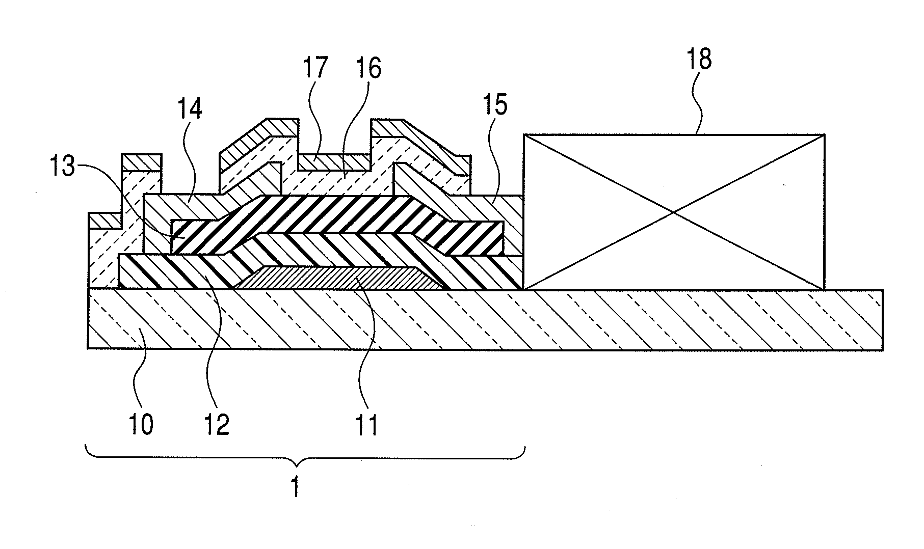
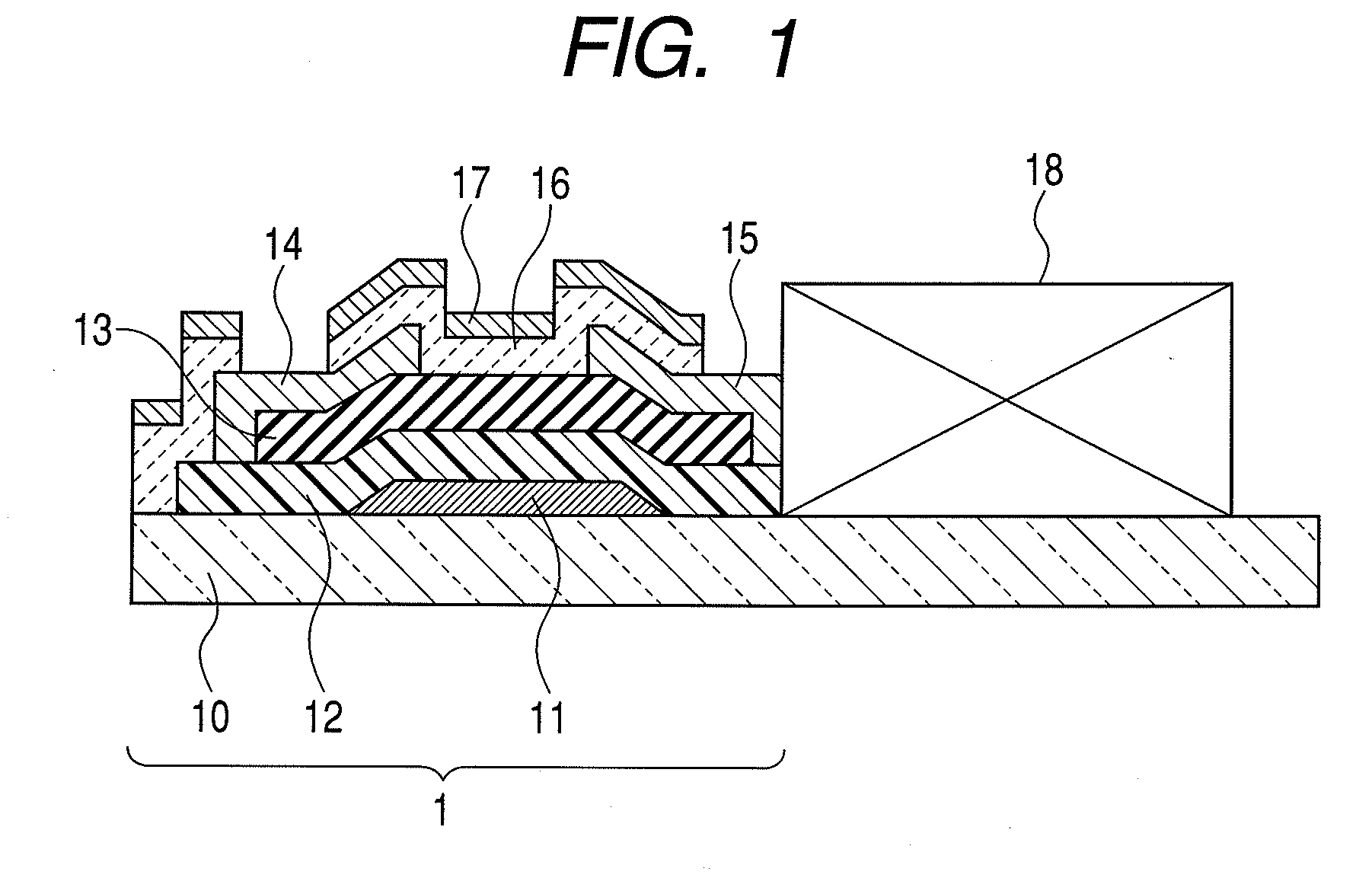
[0061]In this example, an organic EL display device using a-IGZO for a channel layer was fabricated according to the method for manufacturing a semiconductor device and a semiconductor apparatus according to the present invention. In this example, an organic EL device driven at −10 to 30 V was used.

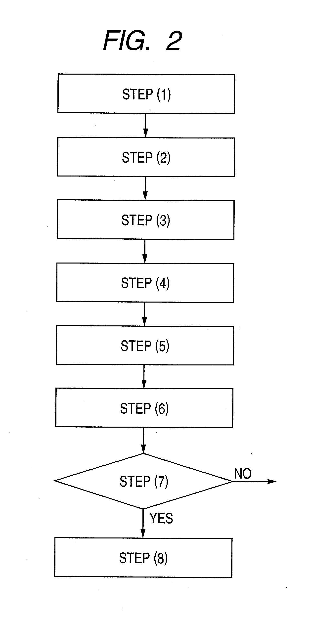
[0062]First, the absorption edge wavelength of a-IGZO was estimated.

[0063]20 nm of an a-IGZO film was formed on an n+-silicon wafer substrate with a thermally oxidized silicon film (film thickness: 100 nm) by a sputtering method. Here, the input RF power was 200 W. Also, for the atmosphere during film formation, the total pressure was 0.5 Pa, and the gas flow ratio at the time was Ar: O2=95:5. Also, the film formation rate was 8 nm / minute, and the substrate temperature was 25° C.

[0064]Next, the phase difference and amplitude ratio of reflected p- and s-polarized light were obtained by ultraviolet-visible spectroscopic ellipsometry. Further, assuming Tauc-Lorentz model absorption and Gauss...


PUM


Abstract

A method for manufacturing a semiconductor device or apparatus having at least a semiconductor as a component, characterized by including irradiating the semiconductor with light having a longer wavelength than the absorption edge wavelength of the semiconductor to change the threshold voltage of the semiconductor device or apparatus, and checking the threshold voltage of the semiconductor device or apparatus, after or during irradiation with the light, to determine whether the threshold voltage is in a predetermined range, during manufacturing the semiconductor device or apparatus.

Description

TECHNICAL FIELD[0001]The present invention relates to a method for manufacturing a semiconductor device or a semiconductor apparatus, and an apparatus for manufacturing the same.BACKGROUND ART[0002]Thin film transistors (TFTs) are widely used as the pixel portions of displays, such as liquid crystal displays and organic EL displays, and the switching devices of drive circuit portions. Currently, aiming at higher TFT performance, lower temperature fabrication process, and lower cost, channel layer materials are searched for and examined among broad types of materials. Such channel layer materials include, for example, amorphous silicon (a-Si), polycrystalline silicon (poly-Si), microcrystalline silicon (μc-Si), and organic semiconductors.[0003]In recent years, amorphous oxide semiconductors have been studied as promising channel layer materials. For example, methods for fabricating TFTs using an amorphous In—Zn—O (described as a-IZO) thin film and an amorphous In—Ga—Zn—O (described a...

Claims


Application Information

Patent Timeline
IPC IPC(8): H01L21/66G21G5/00
CPCH01L22/14H01L29/66969H01L29/7869
Inventor KAJI, NOBUYUKIOFUJI, MASATOTAKAI, YASUYOSHIKAWASAKI, TAKEHIKOKANEKO, NORIOHAYASHI, RYO
Owner CANON KK
Why Eureka
Try Eureka