Method and System for Increasing Alignment Target Contrast

Inactive Publication Date: 2011-03-31
ASML NETHERLANDS BV
View PDF22 Cites 19 Cited by
  • Summary
  • Abstract
  • Description
  • Claims
  • Application Information

AI Technical Summary

Benefits of technology

[0013]In a further embodiment, a first dye or photoactive compound is added to the first resist layer and a second photoactive compound or dye is added to the second resist layer so as to increase optical contrast between the first and second resist layers and to improve diffraction of radiation incident on the alignment mark in the first resist layer.
[0014]According to another embodiment of the present invention, an optical element is provided comprising, a first resist layer having a first optical characteristic and a second resist layer deposited over the first resist layer and having a second optical characteristic. An alignment mark formed by the combination of the first and second resist layers provides enhanced contrast when illuminated with a pre-determined wavelength used for alignment. In an embodiment, one or both of t

Problems solved by technology

However, the alignment mark in the first resist layer may be obliterated or may provide poor contrast and weak di

Method used


Image

  • Method and System for Increasing Alignment Target Contrast
  • Method and System for Increasing Alignment Target Contrast
  • Method and System for Increasing Alignment Target Contrast

Examples


Embodiment Construction

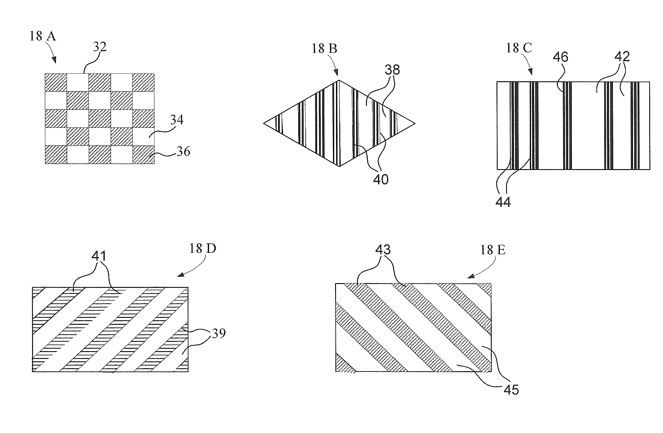
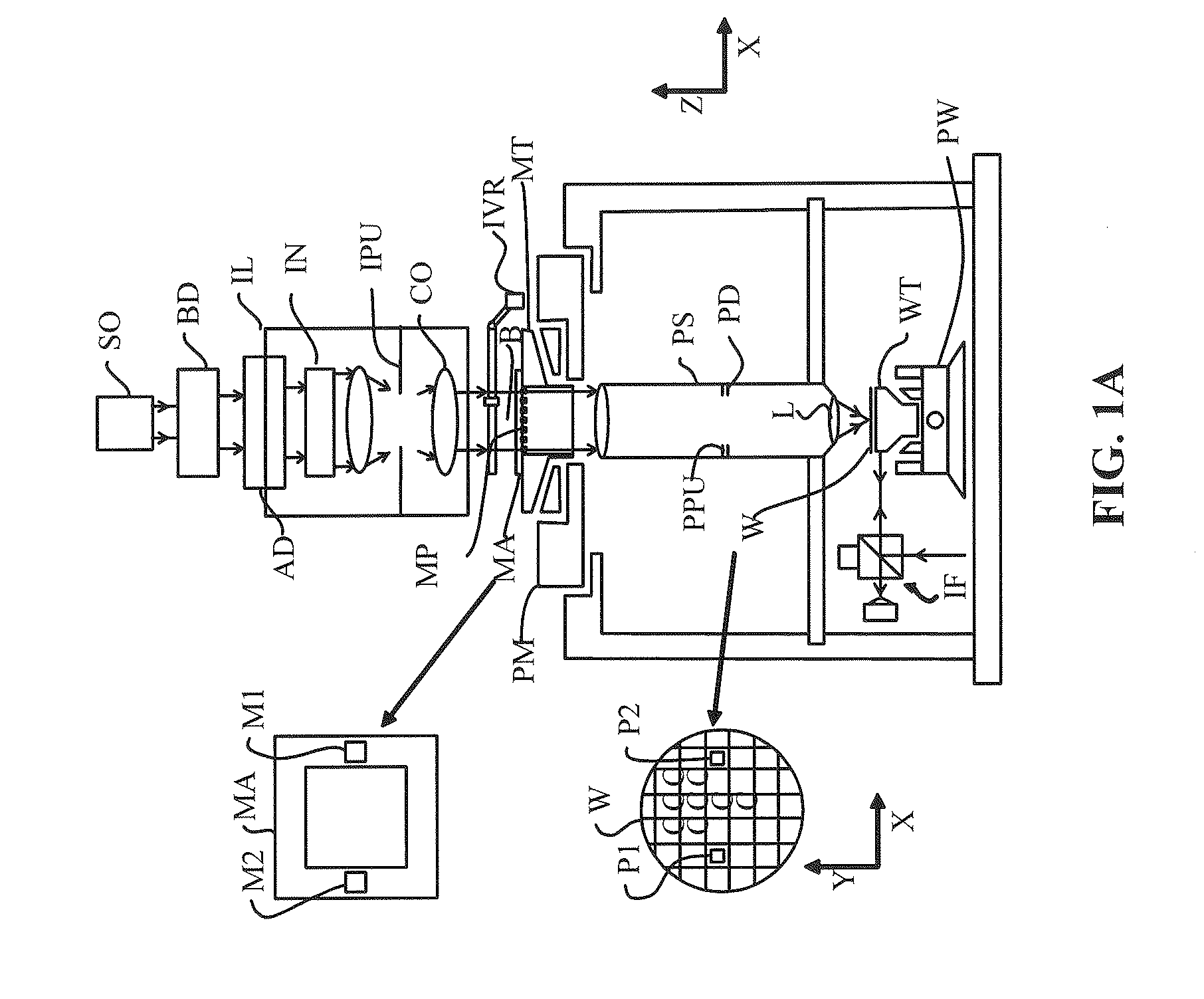
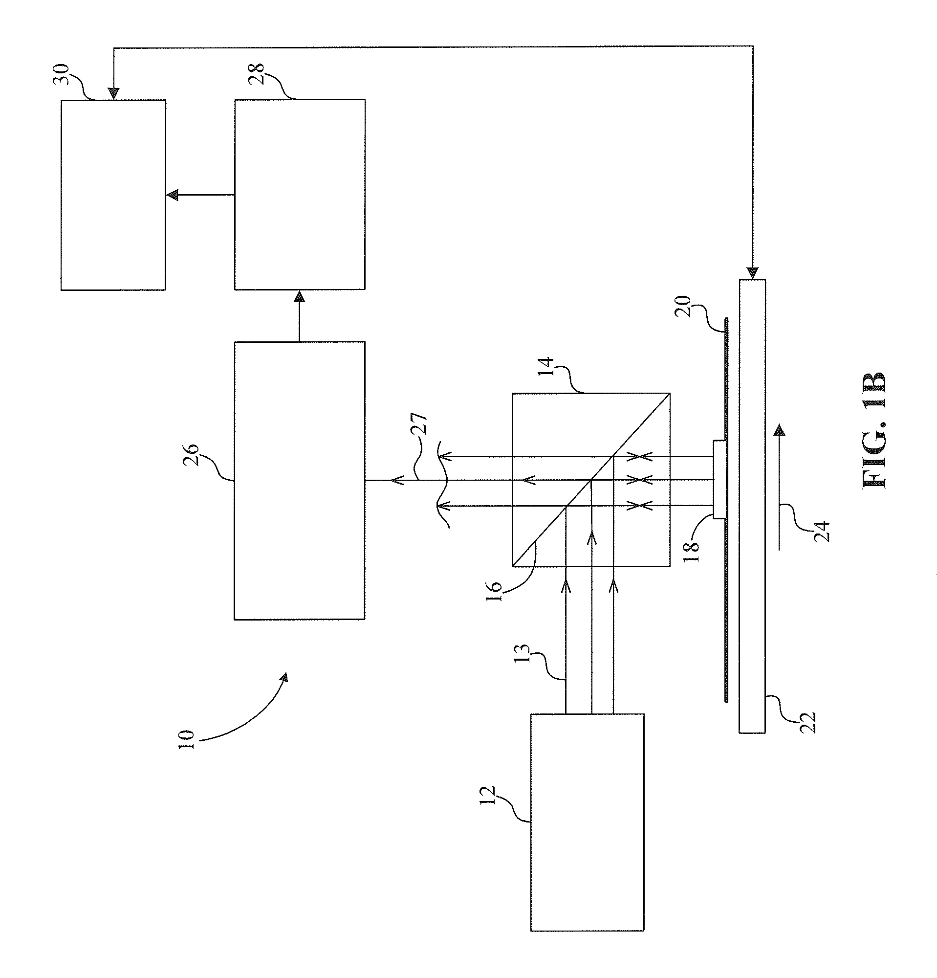
[0030]This specification discloses one or more embodiments that incorporate the features of this invention. The disclosed embodiment(s) merely exemplify the invention. The scope of the invention is not limited to the disclosed embodiment(s). The invention is defined by the claims appended hereto.

[0031]The embodiment(s) described, and references in the specification to “one embodiment”, “an embodiment”, “an example embodiment”, etc., indicate that the embodiment(s) described can include a particular feature, structure, or characteristic, but every embodiment cannot necessarily include the particular feature, structure, or characteristic. Moreover, such phrases are not necessarily referring to the same embodiment. Further, when a particular feature, structure, or characteristic is described in connection with an embodiment, it is understood that it is within the knowledge of one skilled in the art to effect such feature, structure, or characteristic in connection with other embodiment...


PUM


Abstract

A semiconductor wafer is aligned using a double patterning process. A first resist layer having a first optical characteristic is deposited and foams at least one alignment mark. The first resist layer is developed. A second resist layer having a second optical characteristic is deposited over the first resist layer. The combination of first and second resist layers and alignment mark has a characteristic such that radiation of a pre-determined wavelength incident on the alignment mark produces a first or higher order diffraction as a function of the first and second optical characteristics.

Description

CROSS REFERENCE TO RELATED APPLICATION[0001]This application claims the benefit of provisional application 61 / 168,382 filed on Apr. 10, 2009. The subject matter of that application is incorporated herein by reference as if fully set forth herein.BACKGROUND[0002]1. Field of the Invention[0003]The present invention relates generally to an illumination system of the type used in lithographic apparatus for semiconductor wafer manufacture.[0004]2. Related Art[0005]A lithographic apparatus is a machine that applies a desired pattern onto a substrate, usually onto a target portion of the substrate. A lithographic apparatus can be used, for example, in the manufacture of integrated circuits (ICs). In that instance, a patterning device, which is alternatively referred to as a mask or a reticle, may be used to generate a circuit pattern to be formed on an individual layer of the IC. This pattern can be transferred onto a target portion (e.g., comprising part of, one, or several dies) on a sub...

Claims


Application Information

Patent Timeline
IPC IPC(8): G02B5/18G02B5/23G03B27/54G03F7/20
CPCG03F9/7076G03F9/7084G03F9/708
Inventor SEWELL, HARRYDUSA, MIRCEAVAN HAREN, RICHARD JOHANNES FRANCISCUSTENNER, MANFRED GAWEINDOYTCHEVA, MAYA ANGELOVA
Owner ASML NETHERLANDS BV
Why Eureka
Try Eureka