Optical module

a technology of optical modules and wiring devices, applied in the direction of optical elements, lenses, instruments, etc., can solve the problems of increased thickness of lenses is not desired, practical upper limit in thickness, etc., to achieve the effect of improving coupling efficiency and high efficiency of light-collective effect or cos

Inactive Publication Date: 2011-04-07
HITACHI CABLE
View PDF2 Cites 14 Cited by
  • Summary
  • Abstract
  • Description
  • Claims
  • Application Information

AI Technical Summary

Benefits of technology

[0008]However, a conventional technique has a problem in high efficiency of the light-collective effect or cost. For example, in the structure in Patent Document 1, when the vertical cavity surface emitting laser is considered as the surface receiving / emitting element, the light emitted from the vertical cavity surface emitting laser is propagated as spreading. The coupling efficiency is improved by collecting the spread light by the lens and entering the light to the optical transmission path, and therefore, the vertical cavity surface emitting laser and the lens are desirable to be close to each other. This is because the spread of the light emitted from the vertical cavity surface emitting laser is smaller as the vertical cavity surface emitting laser and the lens is closer, and therefore, the light-collective effect required for the lens can be small.
[0010]Generally, the lens having the high light-collective effect is thick. On the other hand, a small scale and flexibility are required for the optical wiring device, and therefore, the increased thickness of the lens is not desired, and a practical upper limit exists in the thickness. Therefore, an upper limit exists even in the light-collective effect, and as a result, there is a possibility that the optical coupling effect is reduced.
[0012]The present invention is made in consideration of the above-described disadvantage points, and an aim of the present invention is to provide means of achieving improvement of optical coupling effect between a surface receiving / emitting element and an optical transmission path with a simple structure and low cost.
[0024]By the optical module according to the typical embodiment of the present invention, the optical wiring device of achieving the high optical coupling efficiency can be provided with low cost and a simple process.

Problems solved by technology

However, a conventional technique has a problem in high efficiency of the light-collective effect or cost.
On the other hand, a small scale and flexibility are required for the optical wiring device, and therefore, the increased thickness of the lens is not desired, and a practical upper limit exists in the thickness.
Therefore, an upper limit exists even in the light-collective effect, and as a result, there is a possibility that the optical coupling effect is reduced.
Therefore, there is a possibility that low cost of the optical wiring is difficult.
Therefore, in the structure, the light-collective effect of the lens is difficult to be improved.

Method used


Image

  • Optical module
  • Optical module
  • Optical module

Examples


first embodiment

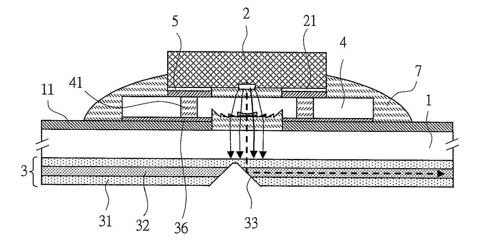
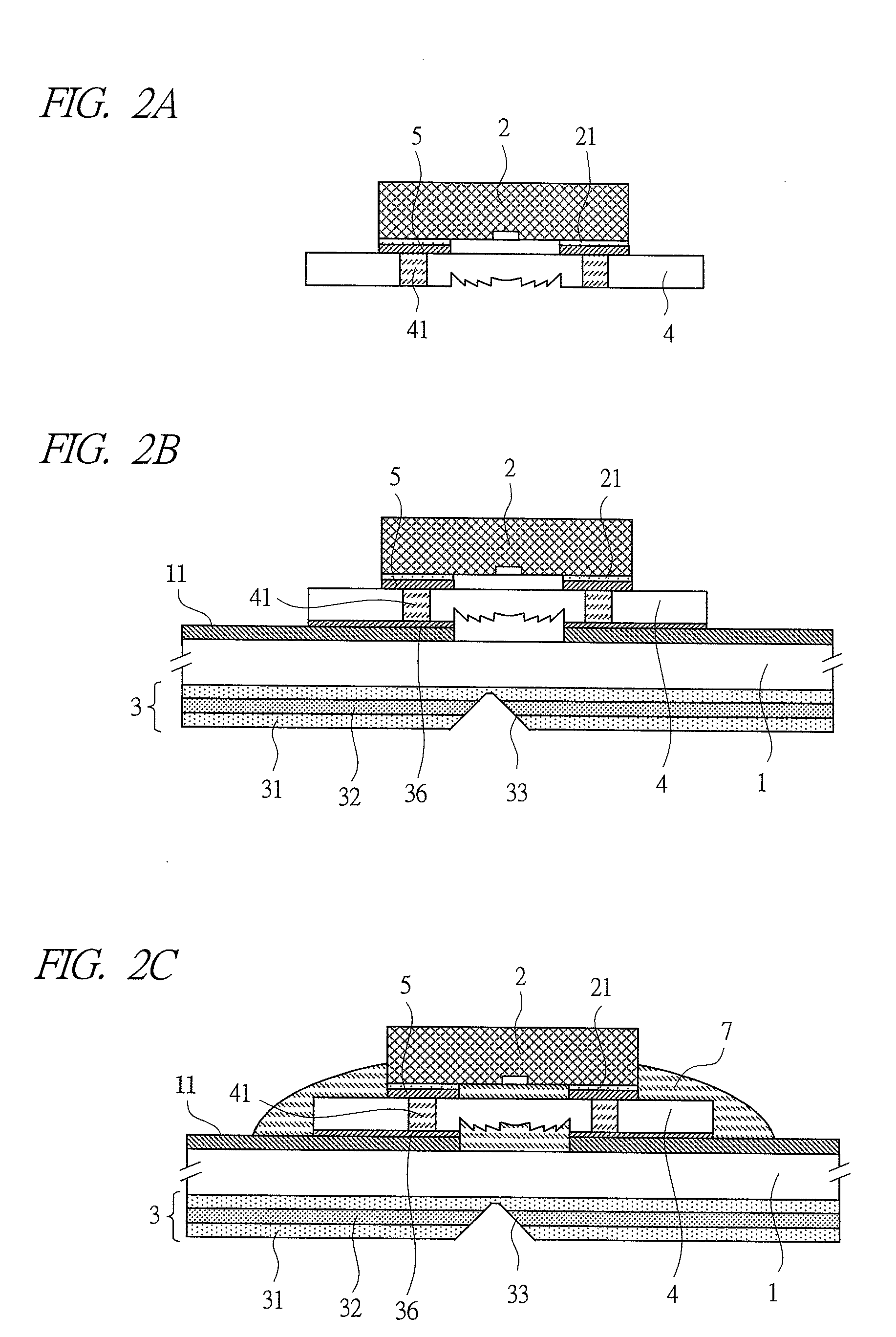
[0048]FIG. 1 is a view of a joint structure between an optical element and a substrate, according to a first embodiment of the present invention. FIGS. 2A to 2C are views describing a joint process according to the first embodiment of the present invention. FIGS. 3A to 3D are views of another joint structure between the optical element and the substrate, according to the first embodiment of the present invention.

[0049]Note that, in FIGS. 1 to 3, it is needless to say that an upper surface of the substrate and a lower surface thereof are not the same cross-sectional view but a developed cross-sectional view. This also goes for embodiments below.

[0050]First, the joint structure of the optical element according to the first embodiment is described with reference to FIG. 1. In FIG. 1, electric wiring 11 is formed on a surface of a substrate 1. In the present embodiment, a flexible substrate made of a polyimide film is used for the substrate 1. Here, a member of the electric wiring 11 ha...

second embodiment

[0090]Next, a second embodiment of the present invention is described with reference to FIGS. 7 to 9.

[0091]FIG. 7 is a cross-sectional view illustrating a joint structure between an optical element and a substrate, according to a second embodiment of the present invention. FIGS. 8A to 8D are views describing a joint process between the optical element and the substrate, according to the second embodiment of the present invention. FIG. 9 is a view describing a structure example of the joint structure between the optical element and the substrate, according to the second embodiment of the present invention.

[0092]Note that, even in the present embodiment, the description is made with using kapton formed of the polyimide film as the substrate 1 and using VCSEL as the optical element 2.

[0093]In the present embodiment, the optical element 2 is directly jointed to the substrate 1. And, a resin lens 45 having a Fresnel lens shape is arranged between the substrate 1 and the optical element 2...

third embodiment

[0109]Next, an example of an optical wiring device using an optical-element joint structure according to this present embodiment is described with reference to FIG. 10. FIG. 10 is a schematic view for describing an optical wiring device using an optical-element joint structure according to a third embodiment of the present invention.

[0110]In this figure, in the electric wiring 11 on an upper surface of the substrate 1, a vertical cavity surface emitting laser (VCSEL) 80, a driver IC 90 for driving the vertical cavity surface emitting laser (VCSEL) 80, a photodiode (PD) 85, and a preamplifier IC 95 for amplifying small signals from the PD 85 with low noises are mounted by flip chip bonding.

[0111]Inside portions corresponding to optical paths between the VCSEL 80 and the substrate 1 and between the PD 85 and the substrate 1, a non-filler content underfill resin 71 is filled. Similarly to the driver IC 90 and the preamplifier IC 95, an underfill resin 72 is filled.

[0112]On a lower surf...


PUM


Abstract

There is provided means of achieving the improvement of optical coupling efficiency between a surface receiving / emitting element and an optical transmission path with a simple structure and low cost. An optical element and a substrate having an optical waveguide layer and electric wiring are connected with each other through a lens having a Fresnel lens shape. A through via is provided in the lens, and the optical element and the electric wiring in the substrate are electrically connected with each other through the through via. Instead of the lens, a unit in which a lens is mounted inside an optical-element mounting substrate may be used.

Description

CROSS-REFERENCE TO RELATED APPLICATION[0001]The present application claims priority from Japanese Patent Application No. 2009-231385 filed on Oct. 5, 2009, the content of which is hereby incorporated by reference into this application.TECHNICAL FIELD OF THE INVENTION[0002]The present invention relates to an optical wiring device of transmitting signals in a substrate, between substrates, between devices, and others with using an optical transmission path, and relates to a method of manufacturing the optical wiring unit.BACKGROUND OF THE INVENTION[0003]In a high-speed transmission wire in recent years, a trend of using a device with optical wiring in place of electric wiring has extended from reasons such as 1) wide band, 2) excellent electromagnetic noise immunity, and 3) light and small volume wiring. In the optical wiring device, as one of the most important factors, there is an optical coupling structure having: an optical element such as a semiconductor laser or a photodiode; an...

Claims


Application Information

Patent Timeline
Patent Type & Authority Applications(United States)
IPC IPC(8): G02B3/08
CPCG02B6/4206G02B6/4214G02B6/43H01L2224/73204H01L2224/32225H01L2924/01327H01L2224/16225H01L2924/00
Inventor TAKAI, TOSHIAKISAKAMOTO, EIJIHATA, SHOHEI
Owner HITACHI CABLE
Why Eureka
Try Eureka