Radiation hardened mos devices and methods of fabrication

a technology of mos circuits and hardening methods, applied in the direction of semiconductor devices, electrical apparatus, transistors, etc., can solve the problems of unintended active parasitic device turning, mos circuits formed using a locos process are not tolerant of ionizing radiation, and trapped charge and interface states, etc., to improve the radiation hardness of the bird's beak region, reduce radiation-induced leakage, and high breakdown voltage

Inactive Publication Date: 2011-04-14
TEXAS INSTR INC
View PDF14 Cites 24 Cited by
  • Summary
  • Abstract
  • Description
  • Claims
  • Application Information

AI Technical Summary

Benefits of technology

[0009]These and other problems associated with the prior art are addressed by the present invention, which provides MOS devices having improved radiation hardness of the bird's beak region by reducing radiation-induced leakage along the bird's beak leakage path while retaining a high breakdown voltage, and methods of fabricating these devices and integrated circuits incorporating them. This is accomplished by doping the bird's beak region to higher levels than permitted previously, specifically in the areas underlying where gate lines cross the bird's beak region, which increases the threshold voltage of the bird's beak region, and by pulling back the source and drain from the edge of the bird's beak into the moat region to increase the breakdown voltage while retaining a predetermined electrical width. A variation of a LOCOS process is used with an additional bird's beak implantation mask as well as alterations to the conventional moat and n-type source / drain masks.

Problems solved by technology

Among the typical issues which must be addressed is the leakage of unintended active parasitic devices turned on by voltage in interconnect lines over the field oxide, which can occur at voltages close to the operating voltage if the doping concentration is low underneath the field oxide.
It is also well known that MOS circuits formed using a LOCOS process are not tolerant of ionizing radiation such as may be encountered in space, in nuclear power plants, or in the vicinity of a nuclear explosion.
When a MOS device is exposed to ionizing radiation, electron-hole pairs are generated in the various oxide regions, resulting in trapped charge and interface states.
Due to the materials involved, the effect is a cumulative buildup of positive charge in the oxide, leading to large negative threshold shifts and thus to leakage particularly in parasitic devices associated with NMOS transistors.
This leakage leads at least to increased power dissipation, and in a worst case can lead to a failure of operation of the device that incorporates the NMOS transistor.
Thinner oxide regions within the isolation region have lower threshold voltages to begin with and are thus most susceptible to this type of leakage.
Increasing the doping of the channel stop to preclude the possibility of radiation-induced inversion layers extending between devices can result in unacceptably low drain-to-substrate breakdown voltages in conventional designs in which the p-type channel stop abuts the n-type source and drain regions.
Moreover, pulling the channel stop away from the moat region to increase breakdown voltage further decreases the dopant concentration in the bird's beak region and the channel region under the gate, leading to increased source-to-drain leakage from these two paths.
Solutions to prevent parasitic leakages between and within devices by simply using higher doping to increase threshold voltages result in decreased breakdown voltages.
Hence, these designs face tradeoffs and are typically significantly larger and / or slower than the unmodified devices.

Method used


Image

  • Radiation hardened mos devices and methods of fabrication
  • Radiation hardened mos devices and methods of fabrication
  • Radiation hardened mos devices and methods of fabrication

Examples


Embodiment Construction

[0026]While the making and using of various embodiments of the present invention are discussed in detail below, it should be appreciated that the present invention provides many applicable inventive concepts that can be embodied in a wide variety of specific contexts. The specific embodiments discussed herein are merely illustrative of specific ways to make and use the invention and do not delimit the scope of the invention.

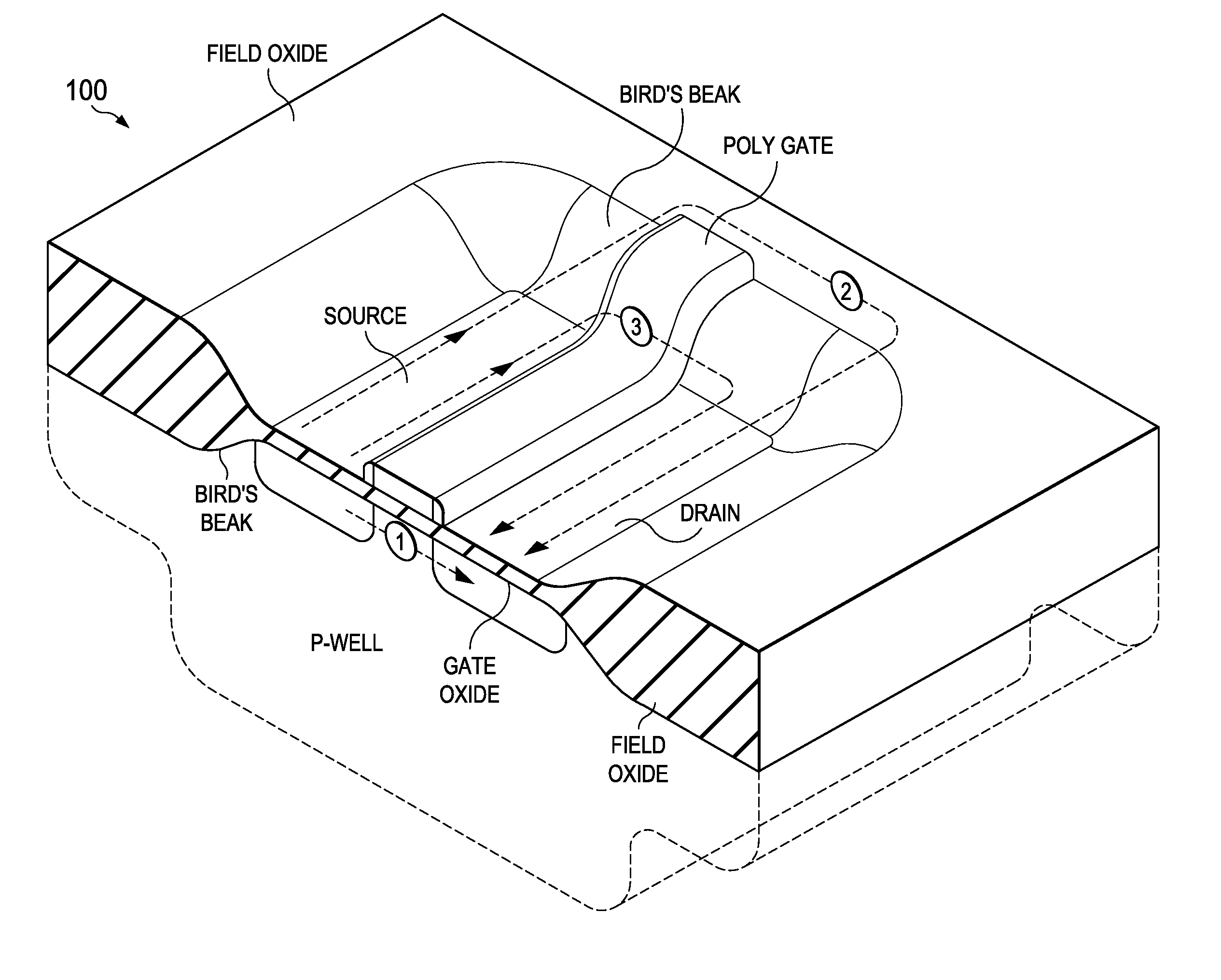
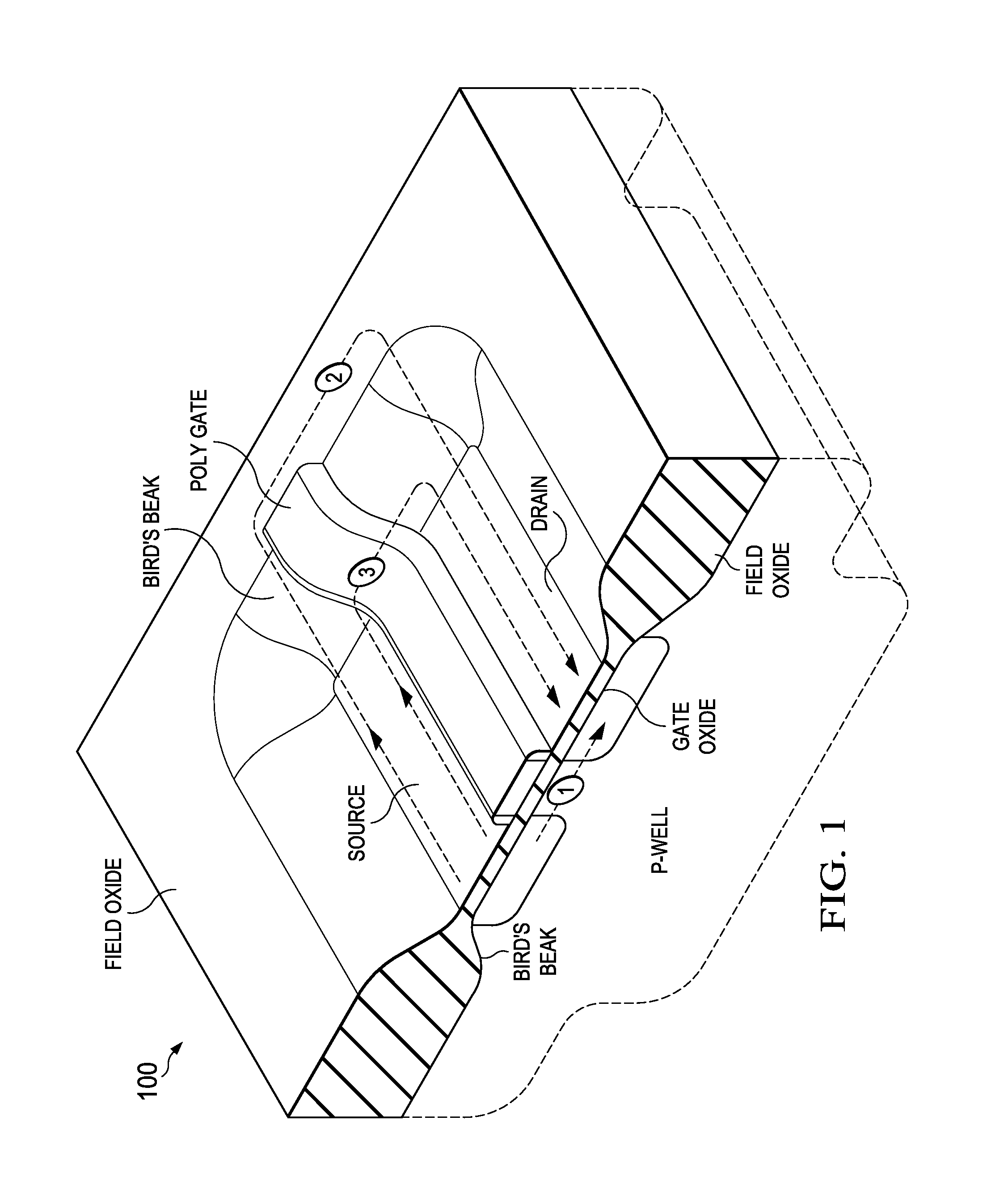
[0027]Referring to FIG. 1, there is shown a cross-sectioned isometric view of a typical NMOS transistor device 100 which can be part of an integrated circuit having multiple such transistors such as an NMOS device, a CMOS device (the PMOS transistor not being shown), or a BiCMOS device (which would additionally include bipolar junction transistors. In the illustrated device, the NMOS transistor is formed in a “p-well” which is a lightly doped p-type region formed within a silicon substrate. Alternatively, an entire top layer several micrometers thick or more of t...


PUM


Abstract

Radiation hardened NMOS devices suitable for application in NMOS, CMOS, or BiCMOS integrated circuits, and methods for fabricating them. A device includes a p-type silicon substrate, a field oxide surrounding a moat region on the substrate tapering through a bird's beak region to a gate oxide within the moat region, a heavily-doped p-type guard region underlying at least a portion of the bird's beak region and terminating at the inner edge of the bird's beak region, a gate crossing the moat region, and n-type source and drain regions spaced by a gap from the inner edge of the guard region. A variation of a local oxidation of silicon process is used with an additional bird's beak implantation mask as well as minor alterations to the conventional moat and n-type source/drain masks. The resulting devices have improved radiation tolerance while having a high breakdown voltage and minimal impact on circuit density.

Description

BACKGROUND OF THE INVENTION[0001]1. Field of the Invention[0002]The present invention relates generally to the field of semiconductor device manufacturing, and more particularly, to variations on the local oxidation of silicon process for isolation of NMOS transistors in integrated circuits having improved radiation hardness and high breakdown voltages.[0003]2. Description of the Related Art[0004]Local oxidation of silicon (LOCOS) fabrication processes are used to provide electrical isolation between devices in integrated circuits (ICs). Variations of such processes are known by several names and may be used to fabricate complementary metal oxide semiconductor (CMOS) as well as n-type metal oxide semiconductor (NMOS) circuits and CMOS circuits incorporating bipolar junction transistors (BiCMOS). In these processes, a thick field oxide is thermally grown in isolation regions between adjacent semiconductor devices that are formed in so-called active or “moat” regions under a thin oxid...

Claims


Application Information

Patent Timeline
Patent Type & Authority Applications(United States)
IPC IPC(8): H01L27/06H01L29/78H01L27/092H01L21/8238H01L21/8249H01L21/762
CPCH01L21/2652H01L29/78H01L21/823878H01L21/76202
Inventor DONNELLY, EMILY ANNBURGESS, BYRON NEVILLEKAHN, RANDOLPH W.STUBBLEFIELD, TODD DOUGLAS
Owner TEXAS INSTR INC
Why Eureka
Try Eureka