Reflecting light emitting structure and method of manufacture thereof

a light-emitting structure and fabrication method technology, applied in the direction of semiconductor/solid-state device manufacturing, electrical equipment, semiconductor devices, etc., can solve the problems of requiring efficient and expensive packaging, and the relative complexity of packaging is required to achieve the effect of reducing mechanical strain

Active Publication Date: 2011-05-05
QORVO US INC
View PDF25 Cites 17 Cited by
  • Summary
  • Abstract
  • Description
  • Claims
  • Application Information

AI Technical Summary

Benefits of technology

[0005]The present disclosure provides a reflecting light emitting structure and method of manufacture that incorporates a silicon (Si) substrate having a uniformly textured surface. Light emissions from a light emitting diode (LED) are efficiently scattered by the uniformly textured surface of the Si substrate. The light reflecting structure of the present disclosure is particularly well suited for efficiently reflecting light generated by a gallium nitride (GaN) LED that emits blue light.
[0006]The disclosed reflecting light emitting structure includes a substrate having a first face and a second face, wherein the first face is in a first crystallographic plane. A plurality of grooves is formed in the first face of the substrate, wherein each of the plurality of grooves includes a first sidewall that is coplanar with a second crystallographic plane and a second sidewall that is coplanar with a third crystallographic plane. A buffer layer is provided on the substrate to reduce mechanical strain between the substrate and an LED fabricated on the buffer layer.

Problems solved by technology

However, relatively complex and expensive packaging is required to efficiently scatter light emissions from a GaN LED structure.

Method used


Image

  • Reflecting light emitting structure and method of manufacture thereof
  • Reflecting light emitting structure and method of manufacture thereof
  • Reflecting light emitting structure and method of manufacture thereof

Examples


Embodiment Construction

[0015]The embodiments set forth below represent the necessary information to enable those skilled in the art to practice the disclosure and illustrate the best mode of practicing the disclosure. Upon reading the following description in light of the accompanying drawing figures, those skilled in the art will understand the concepts of the disclosure and will recognize applications of these concepts not particularly addressed herein. It should be understood that these concepts and applications fall within the scope of the disclosure and the accompanying claims.

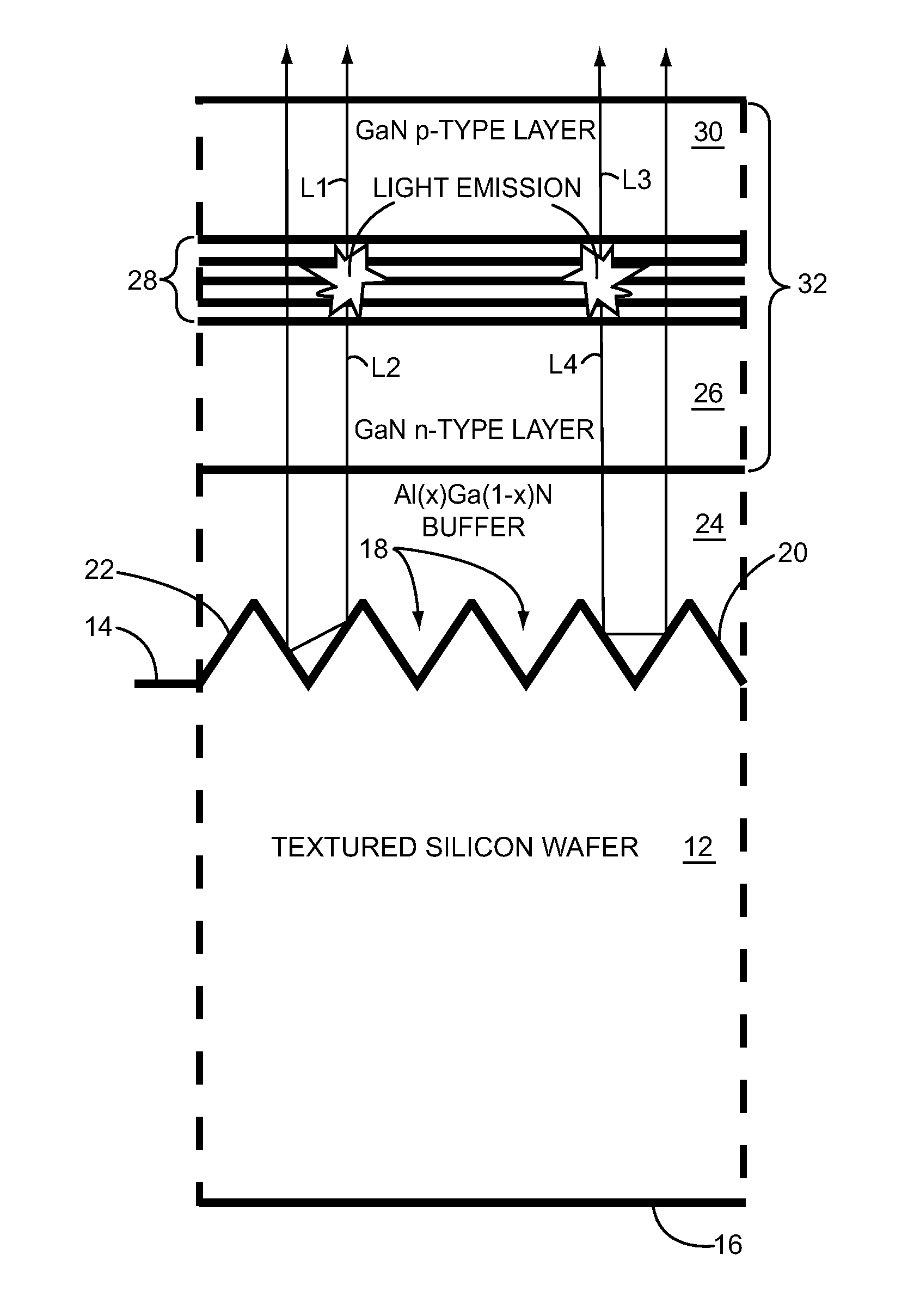
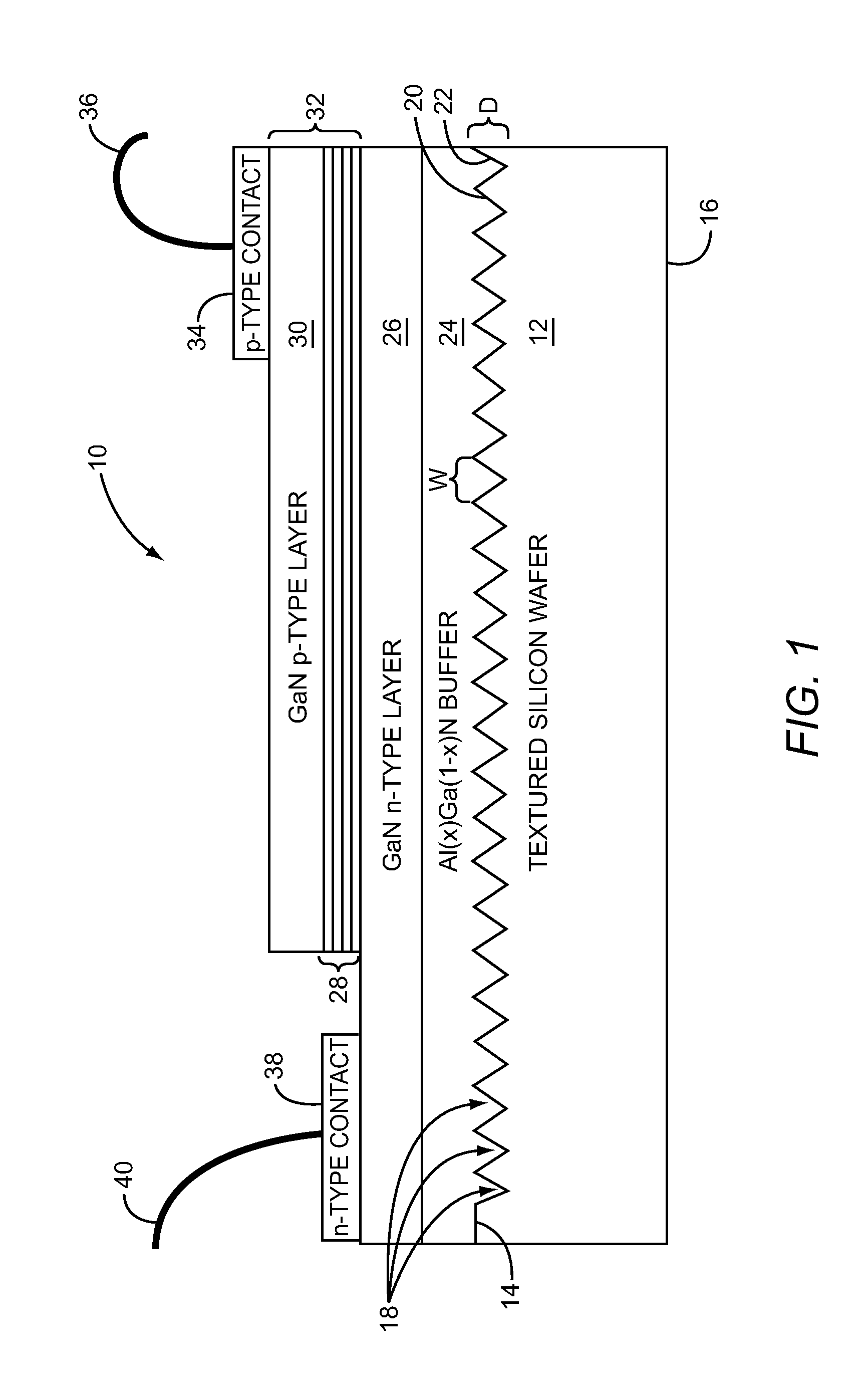
[0016]FIG. 1 provides a cross-section view of one embodiment of a reflecting light emitting structure 10 according to the present disclosure. The reflecting light emitting structure 10 includes a substrate 12 having a first face 14 and a second face 16. The substrate 12 is preferably made of a material that has a uniform crystalline structure. A silicon (Si) wafer like those commonly used in integrated circuit manufacturing is ...


PUM


Abstract

A reflecting light emitting structure includes a substrate having a plurality of grooves formed in a first face of the substrate is disclosed. The first face is in a first crystallographic plane. Each of the plurality of grooves includes a first sidewall that is coplanar with a second crystallographic plane and a second sidewall that is coplanar with a third crystallographic plane. A buffer layer is provided on the substrate to reduce mechanical strain between the substrate and a light emitting diode (LED) fabricated on the buffer layer.

Description

RELATED APPLICATIONS[0001]This application claims the benefit of provisional patent application Ser. No. 61 / 227,630, filed Jul. 22, 2009, the disclosure of which is hereby incorporated herein by reference in its entirety. The application also relates to provisional patent application Ser. No. 61 / 227,624, filed Jul. 22, 2009, and to utility patent application Ser. No. 12 / 705,869 filed Feb. 15, 2010, both of which are hereby incorporated herein by reference in their entireties.FIELD OF THE DISCLOSURE[0002]The present disclosure relates to a structure and fabrication method for a reflecting light emitting structure that includes a textured substrate, and in particular to a textured substrate having uniform grooves.BACKGROUND OF THE DISCLOSURE[0003]Prior art solid state lighting systems use gallium nitride (GaN) that is grown on 150 millimeter (mm) silicon (Si) wafers. Light extraction efficiency is often improved for light emitting diodes (LEDs) grown on sapphire or silicon carbide (Si...

Claims


Application Information

Patent Timeline
Patent Type & Authority Applications(United States)
IPC IPC(8): H01L33/04H01L33/12
CPCH01L33/22H01L27/15H01L2224/49107
Inventor O'KEEFE, MATTHEW FRANCIS
Owner QORVO US INC
Why Eureka
Try Eureka