Output current detecting circuit and transmission circuit

a current detection and output technology, applied in the field of output current detecting circuits, can solve the problems of large large power consumption of devices, and apprehend device breakage, so as to improve judgment accuracy of comparison circuits, reduce power loss of sensing resistors, and prevent output transistor breakage caused by excess current

Active Publication Date: 2011-05-19
MITSUMI ELECTRIC CO LTD
View PDF12 Cites 9 Cited by
  • Summary
  • Abstract
  • Description
  • Claims
  • Application Information

AI Technical Summary

Benefits of technology

[0012]The present invention was made in view of the aforesaid problem, and aims to provide an output current detecting circuit capable of suppressing the power loss in a sensing resistor and thereby suppressing the rise of a chip temperature and a transmission circuit equipped with the output current detecting circuit.
[0013]Another object of the present invention is to provide an output current detecting circuit made as a semiconductor integrated circuit capable of reducing the occupation area of the output circuit thereof, the chip size by extension and a transmission circuit equipped with the output current detecting circuit.
[0022]According to the configuration described above, if the size of the current detecting transistor is set to 1 / N of the size of the output transistor, an output current value can be detected only by flowing a current into the first resistance element as the sensing resistor connected in series with the current detecting transistor, the magnitude of which current is 1 / N of the current flowing through the output transistor, and consequently the power loss of the sensing resistor can greatly be reduced. Furthermore, because the configuration generates the reference voltage based on the power source voltage, a relative judgment level does not change even if the power source voltage changes, and the judgment accuracy of the comparison circuit can be improved.
[0024]Furthermore, preferably, the output current detecting circuit is configured to further comprises a first MOS transistor connected between the constant current circuit and the second resistance element, the first MOS transistor having a gate terminal to which a voltage same as that applied to a gate terminal of the current detecting transistor is applied. Hereby, if a drain current (detection current) changes owing to a change of the drain-source voltage of a current detecting MOS transistor caused by a change of the power source voltage, the drain-source voltage of the first MOS transistor, having the gate terminal to which the voltage same as the gate voltage of the current detecting MOS transistor is applied, is similarly changes, and consequently the changes of the drain current can be made to have the same characteristic to enable the changes of the current flowing through the second resistance element and further the changes of the reference voltage to be small.
[0037]According to the configuration described above, a current flowing through the sensing resistor can be made to be small, and thereby the power loss of the sensing resistor can greatly be made to be reduced. Furthermore, if a current equal to or more than a predetermined value flows through the output transistor, the current is detected and the output transistor is turned off. Thereby, the breakage of the output transistor caused by an excess current can be prevented. Furthermore, because the configuration generates the reference voltage based on the power source voltage, the relative judgment level does not vary if the power source voltage varies, and the judgment accuracy of the comparison circuit can be improved.
[0038]According to the present invention, the following effects can be obtained. An output current detecting circuit capable of suppressing the power loss of a sensing resistor to suppress the rise of a chip temperature and a transmission circuit equipped with the output current detecting circuit can be realized. Furthermore, an output current detecting circuit made to be a semiconductor integrated circuit capable of reducing the occupation area of an output circuit, a chip size by extension, and a transmission circuit equipped with the output current detecting circuit can be realized. Furthermore, an output current detecting circuit having low power source voltage dependency and low temperature dependency and a transmission circuit equipped with the output current detecting circuit can be realized.

Problems solved by technology

Because a relatively large current flows through the current detecting resistor Rs (hereinafter referred to as a sensing resistor) provided in series with the output transistor Q1 in the output current detecting circuit of FIG. 6, the power loss thereof is large and the power consumption thereof becomes much.
Consequently, when a chip temperature rises owing to the heat generation of the sensing resistor Rs to exceed a package allowable temperature, it is apprehended that the device is broken.
Although the power loss of the sensing resistor Rs can be reduced, here, by using a low resistance element, it is difficult by the present process technique to obtain a highly accurate low resistance element on a semiconductor chip on which the output current detecting circuit is formed, and, if the resistance value of the sensing resistor Rs disperses, an excess current detection level results in dispersing.
Furthermore, because the p-channel type MOS transistor, having a device size larger than that of the n-channel type MOS transistor of the same drive power, is used as the output transistor Q1 in the output current detecting circuit of FIG. 6, the output current detecting circuit has the problem in which the occupation area of the output circuit, the chip size thereof by extension, is large.

Method used


Image

  • Output current detecting circuit and transmission circuit
  • Output current detecting circuit and transmission circuit
  • Output current detecting circuit and transmission circuit

Examples


first embodiment

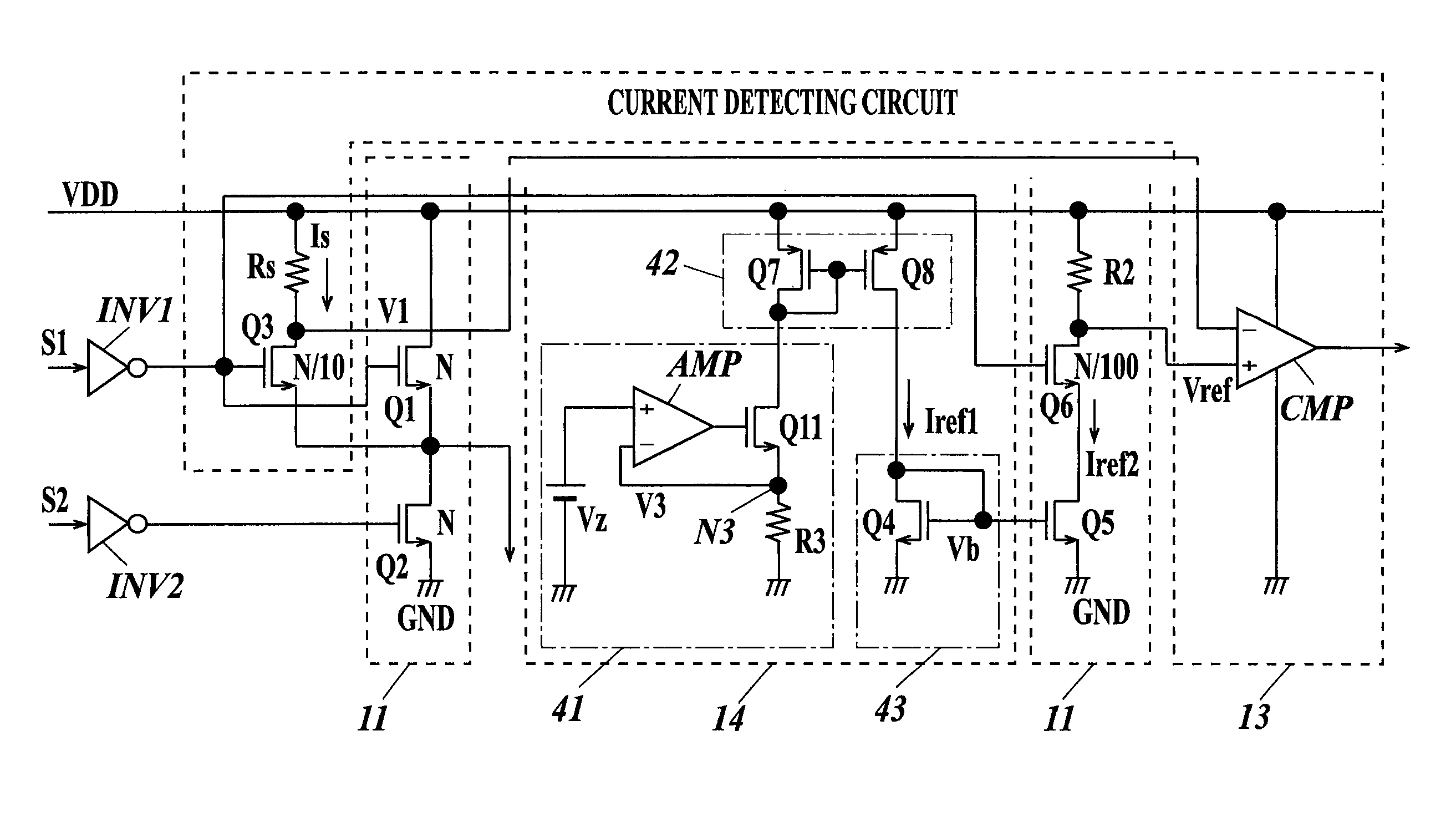
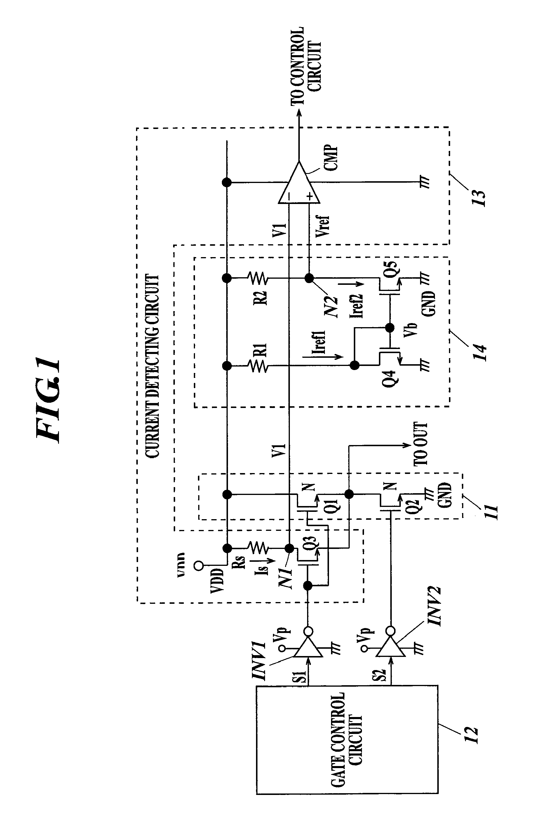
[0047]FIG. 1 shows a transmission circuit to be incorporated in an home bus system (HBS) driver / receiver IC mounted in a piece of equipment constituting a system to which the HBS is applied, the HBS driver / receiver IC bearing the communication function between pieces of equipment. In addition, FIG. 1 shows a circuit on one side of driving one of twisted-pair lines, and a real transmission circuit of the IC is provided with one more circuit as shown in FIG. 1 for outputting an AMI-coded signal having a different polarity.

[0048]The transmission circuit of the present embodiment is equipped with output transistors Q1 and Q2 connected in series with each other between a power source voltage terminal VDD and a ground potential point GND; the output drive circuit 11 as a push-pull type output circuit, which drives the transmission line to output an AMI-coded data signal; the gate control circuit 12 generating control signals S1 and S2 for performing the on-off control of the transistors Q...

second embodiment

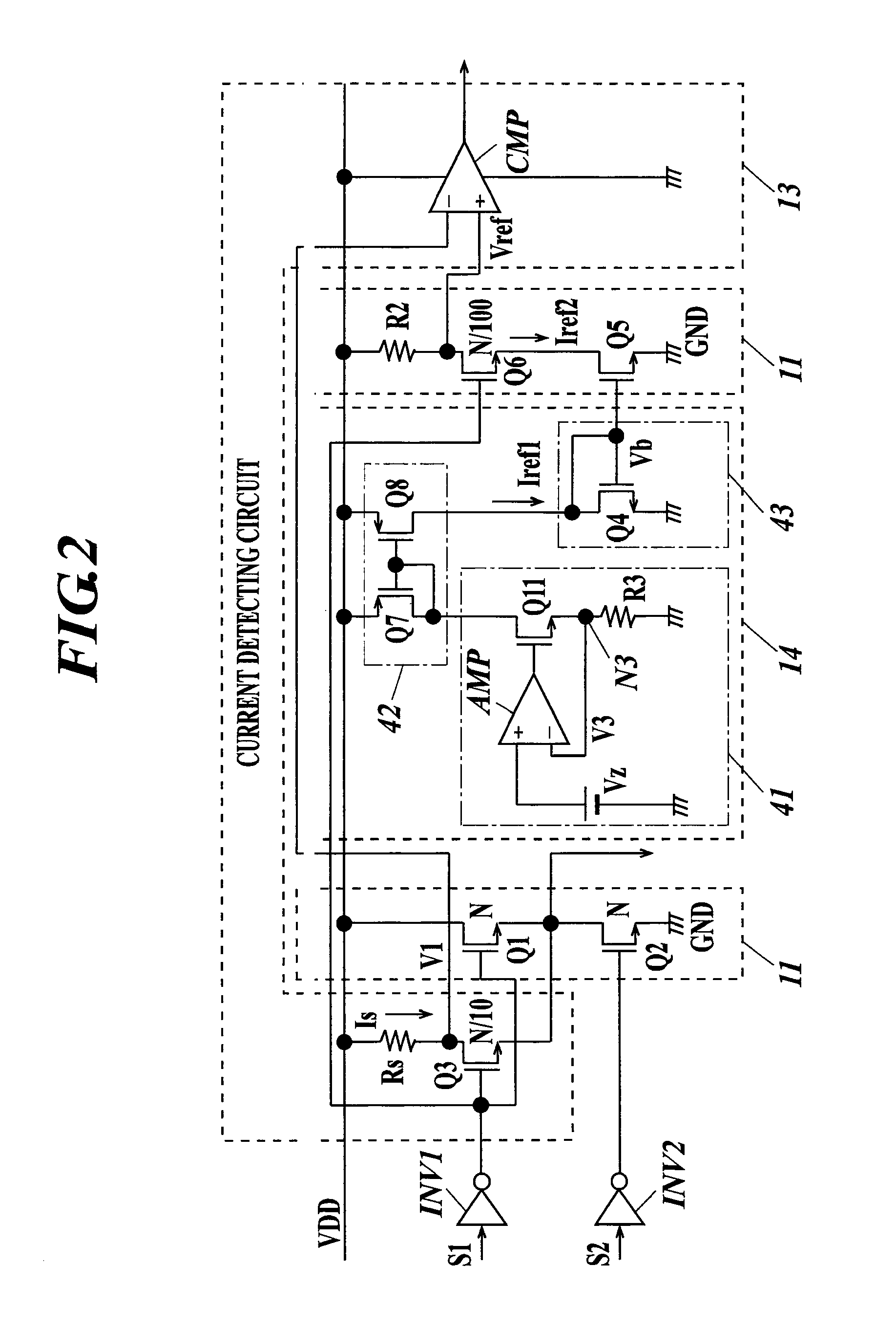
[0058]Next, a transmission circuit equipped with a reference voltage generating circuit having improved power source voltage dependency and improved temperature dependency will be described.

[0059]FIG. 2 shows the transmission circuit of the second embodiment. In the present embodiment, a MOS transistor Q6 having a gate terminal, to which a voltage same as that applied to the gate terminal of the MOS transistor Q3 in the output current detecting circuit 13 is applied, is serially connected between the resistor R2 generating the reference voltage Vref by its voltage drop and the MOS transistor Q5 generating the current Iref2 flowing through the resistor R2.

[0060]Furthermore, the reference voltage generating circuit 14 is equipped with a constant current source circuit 41 including an operational amplifier AMP having a non-inverting input terminal, to which a standard voltage source Vz having no temperature characteristics is connected; a cascode type current mirror circuit 42 flowing ...


PUM


Abstract

An output current detecting circuit includes: a current detecting transistor having a size smaller than that of an output transistor and a control terminal, to which a voltage same as a control voltage of the output transistor is applied; a sensing resistor connected to the current detecting transistor in a serial mode; a comparison circuit comparing a voltage converted by the sensing resistor and a reference voltage to judge a magnitude of a current flowing through the output transistor; and a reference voltage generating circuit, wherein the reference voltage generating circuit includes a constant current circuit flowing a constant current and a resistance element having one terminal connected to a power source voltage terminal, the reference voltage generating circuit generating the reference voltage based on a power source voltage by the conversion of the constant current into a voltage by flowing the constant current through the resistance element.

Description

BACKGROUND OF THE INVENTION[0001]1. Field of the Invention[0002]The present invention relates to an output current detecting circuit losing little electric power, an output current detecting circuit being scarcely influenced by power supply voltage variations and temperature variations, and a transmission circuit equipped with one of the output current detecting circuits.[0003]2. Description of Related Art[0004]A home bus system (HBS) exists as a communication standard between household electrical appliances. The HBS includes a standard regulating the use of twisted-pair lines for a transmission path and the use of an alternate mark inversion (AMI) coded signal (hereinafter referred to as an AMI signal) for the transmission of a digital signal on the transmission path. An AMI signal is composed of three values of zero, plus, and minus, and data is transmitted in the way of expressing logic “0” by a zero and logic “1” by alternating the polarity of the signal in communication using t...

Claims


Application Information

Patent Timeline
Patent Type & Authority Applications(United States)
IPC IPC(8): H02M11/00
CPCG05F1/573
Inventor OHARA, TOMOMITSUGOTO, TAKAFUMI
Owner MITSUMI ELECTRIC CO LTD
Why Eureka
Try Eureka