Method for reducing line width roughness with plasma pre-etch treatment on photoresist

a pre-etch treatment and plasma technology, applied in the direction of electrical discharge tubes, decorative arts, electrical equipment, etc., can solve the problems of line edge roughness (ler) and variation, affecting the quality of plasma pre-etching, etc., to achieve the effect of reducing the line width roughness of a featur

Inactive Publication Date: 2011-05-19
LAM RES CORP
View PDF5 Cites 360 Cited by
  • Summary
  • Abstract
  • Description
  • Claims
  • Application Information

AI Technical Summary

Benefits of technology

[0006]To achieve the foregoing and in accordance with the purpose of the present invention, a method for reducing line width roughness (LWR) of a feature in an etch layer below a patterned photoresist mask having mask features is provided. The method includes (a) non-etching plasma pre-etch treatment of the photoresist mask, and (b) etching of a feature in the etch layer through the pre-treated photoresist mask using an etching gas. The non-etching plasma pre-etch treatment includes (a1) providing a treatment gas containing H2 and COS, (a2) forming a plasma from the treatment gas, and (a3) stopping the treatment gas.

Problems solved by technology

Poor and distorted line edges, as well as incompletely developed residue of photoresist layer will cause significant roughness at the edges of line and space features causing line edge roughness (LER) and variation in the CD of the line and space features, i.e., line width roughness (LWR).
This non-uniform edge pattern will be transferred and / or amplified during multiple etch process steps that are required for semiconductor device fabrication, causing degradation of device performance and yield loss.
However, for various reasons as described above, the actual line feature may appear jagged and have line width roughness (LWR).
Features with high LWR are generally very undesirable because the CD measured along the line feature would vary from position to position, rendering operation of the resulting device unreliable.

Method used


Image

  • Method for reducing line width roughness with plasma pre-etch treatment on photoresist
  • Method for reducing line width roughness with plasma pre-etch treatment on photoresist
  • Method for reducing line width roughness with plasma pre-etch treatment on photoresist

Examples


Embodiment Construction

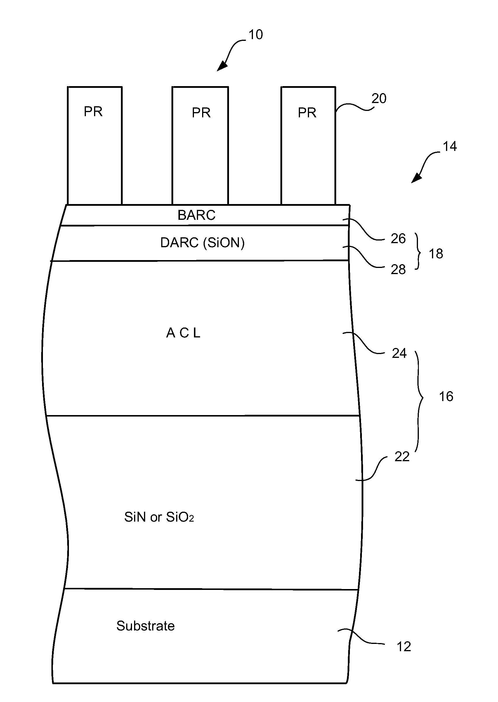
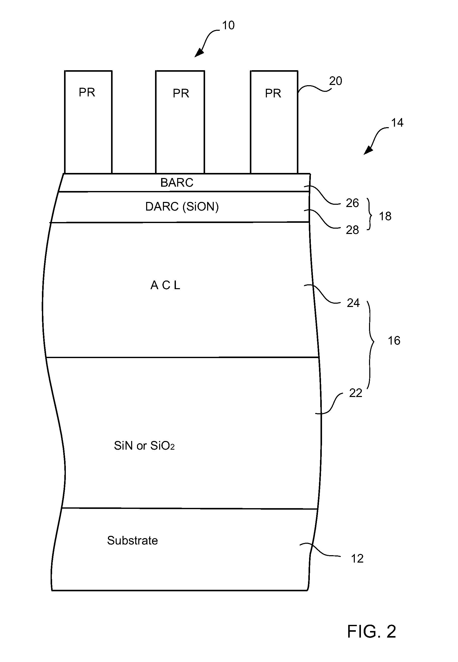
[0022]The present invention will now be described in detail with reference to a few preferred embodiments thereof as illustrated in the accompanying drawings. In the following description, numerous specific details are set forth in order to provide a thorough understanding of the present invention. It will be apparent, however, to one skilled in the art, that the present invention may be practiced without some or all of these specific details. In other instances, well known process steps and / or structures have not been described in detail in order to not unnecessarily obscure the present invention.

[0023]To facilitate understanding, FIG. 2 is a schematic cross-sectional view of an example of a wafer stack 10 for front end of line (FEOL) applications such as dielectric material etch in which embodiments of the present invention may be applied. The wafer stack 10 includes a substrate 12 and a stack of layers 14 formed on the substrate 12. As shown in FIG. 2, the stack of layers 14 incl...


PUM

PropertyMeasurementUnit
thicknessaaaaaaaaaa
bias voltageaaaaaaaaaa

Abstract

A method for reducing line width roughness (LWR) of a feature in an etch layer below a patterned photoresist mask having mask features is provided. The method includes (a) non-etching plasma pre-etch treatment of the photoresist mask, and (b) etching of a feature in the etch layer through the pre-treated photoresist mask using an etching gas. The non-etching plasma pre-etch treatment includes (a1) providing a treatment gas containing H2 and COS, (a2) forming a plasma from the treatment gas, and (a3) stopping the treatment gas.

Description

BACKGROUND OF THE INVENTION[0001]The present invention relates to reducing line width roughness (LWR) of a feature of an etch layer. More specifically, the present invention relates to a plasma pre-etch treatment of a patterned photoresist mask through which a feature is to be etched in an underlying etch layer.[0002]During semiconductor wafer processing, features of the semiconductor device are defined in the wafer using well-known patterning and etching processes. In these processes (photolithography), a photoresist (PR) material may be deposited on the wafer and then is exposed to light filtered by a reticle. The reticle may be a transparent plate that is patterned with exemplary feature geometries that block light from propagating through the reticle.[0003]After passing through the reticle, the light contacts the surface of the photoresist material. The light changes the chemical composition of the photoresist material such that a developer can remove a portion of the photoresis...

Claims


Application Information

Patent Timeline
Patent Type & Authority Applications(United States)
IPC IPC(8): H01L21/306C23F1/08
CPCH01J37/32091H01L21/0338H01J37/32935
Inventor SHEU, BEN-LISHIM, MARTINKIM, JONATHAN
Owner LAM RES CORP
Why Eureka
Try Eureka