Porous silicon electro-etching system and method

a technology of porous silicon and electro-etching, which is applied in the direction of sustainable manufacturing/processing, manufacturing tools, and final product manufacturing, etc., can solve the problems of preventing competing c-si pv technologies from reaching grid-parity costs, using extensive and costly process steps, and inherent cost of semiconductor-grade silicon substrates, etc., to achieve the effect of improving the electrical field and improving the distribution of porous silicon

Active Publication Date: 2011-05-26
TRUTAG TECH +1
View PDF99 Cites 14 Cited by
  • Summary
  • Abstract
  • Description
  • Claims
  • Application Information

AI Technical Summary

Benefits of technology

[0067]The present disclosure provides an electro-etching system which consists of conveyorized transport of wafer-holding pallets, in which the pallets form an integral and critical functional component of the electrolytic cell and a means of sealing a silicon wafer solely from the backside of the wafer. This sealing allows the prevention of shadowing, blocking, and exclusion zones on the wafer frontside. The pallets also provide transport from wafer loading to wafer un-loading through the electro-etching system. The pallets are a component of some embodiments of the present disclosure, but they are not a necessary component of all embodiments.
[0068]The transition from a single-wafer sealed cylindrical chamber in known systems to the newly presented in-line immersion configuration may result in a significant increase in the electrical field and an improved porous silicon distribution across the surface of the wafer in process.
[0069]The pallet and conveyor

Problems solved by technology

In the solar cell industry, known high-efficiency technologies usually use semiconductor-grade mono-crystalline silicon wafers, produced using extensive and costly process steps.
The inherent cost of semicon

Method used


Image

  • Porous silicon electro-etching system and method
  • Porous silicon electro-etching system and method
  • Porous silicon electro-etching system and method

Examples


Embodiment Construction

[0033]The following description is not to be taken in a limiting sense, but is made for the purpose of describing the general principles of the present disclosure. The scope of the present disclosure should be determined with reference to the claims. Exemplary embodiments of the present disclosure are illustrated in the drawings, like numbers being used to refer to like and corresponding parts of the various drawings.

[0034]The present disclosure presents a PV cell substrate fabrication process flow using porous silicon as a sacrificial layer.

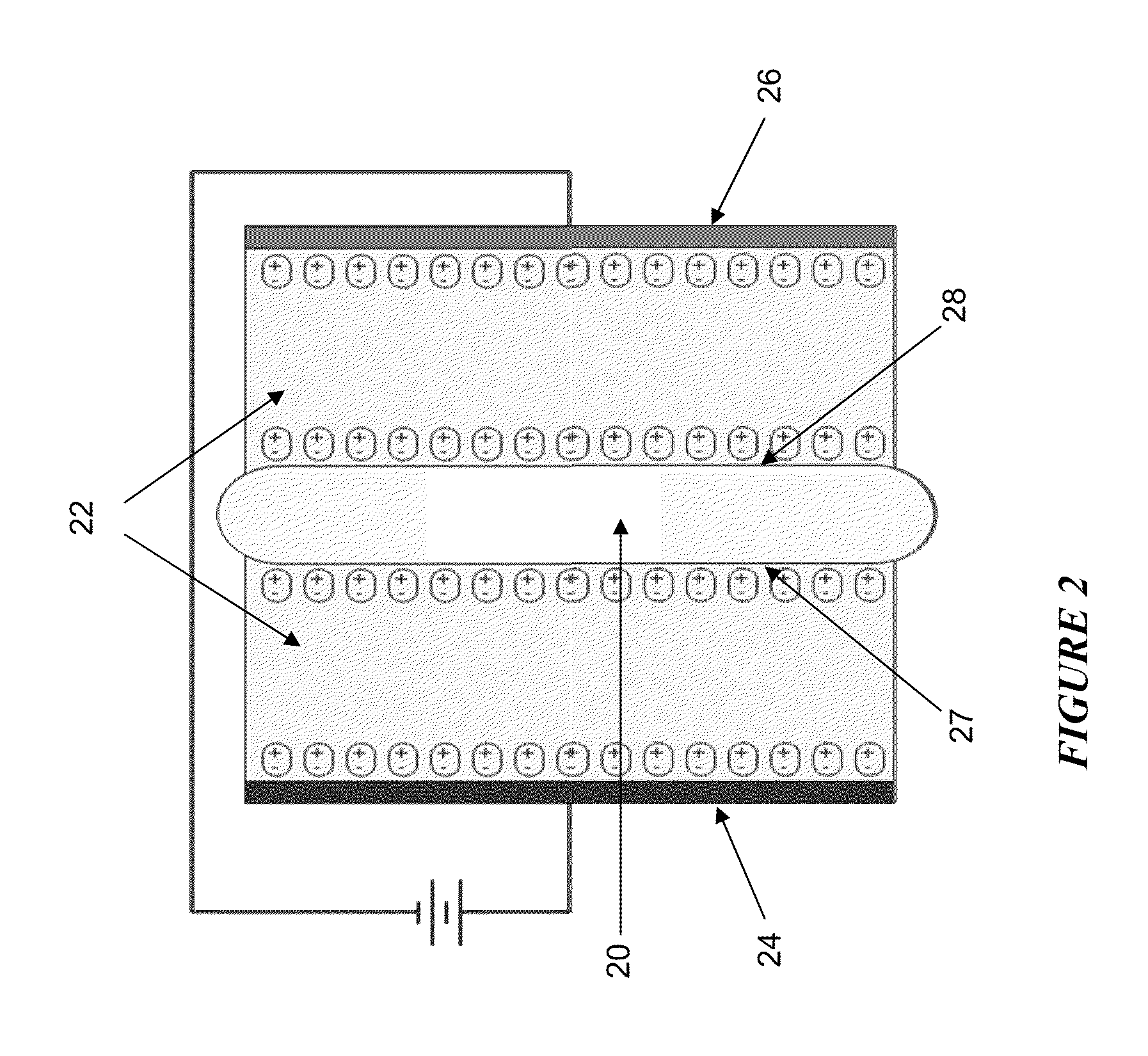
[0035]The system may produce porous silicon films with acceptable quality for supporting the manufacturing of PV cells. FIGS. 1-6 relate generally to production of PV cells.

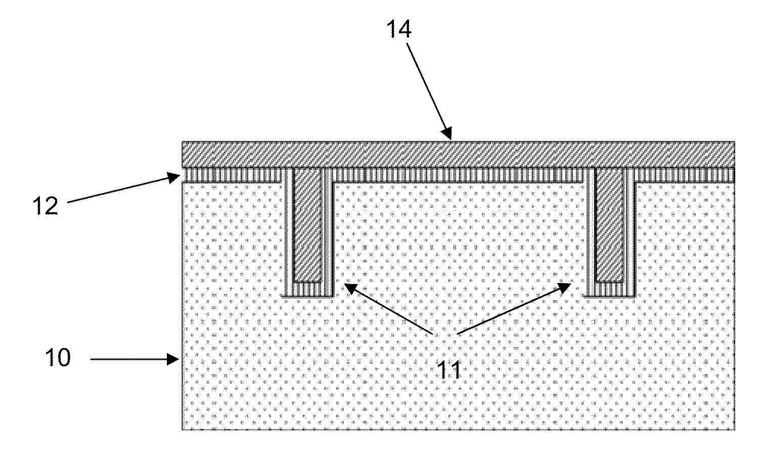
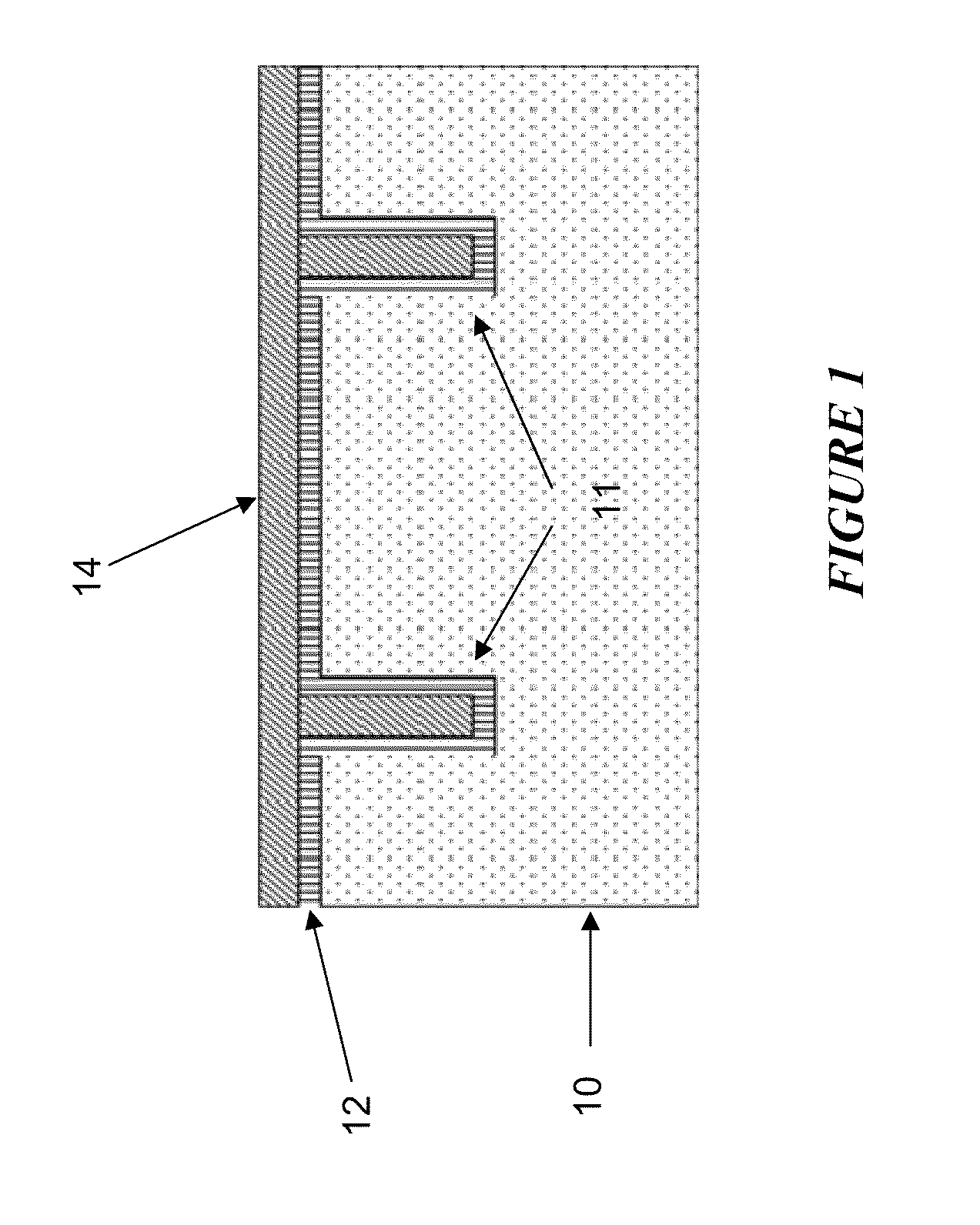
[0036]FIG. 1 shows a step in the process of creating a solar cell using the sacrificial porous silicon release layer of the present disclosure. Bulk p-type silicon wafer 10 has had trenches 11 patterned into it, for example by deep reactive-ion etching (DRIE) or by chemical e...


PUM


Abstract

It is an object of this disclosure to provide high productivity, low cost-of-ownership manufacturing equipment for the high volume production of photovoltaic (PV) solar cell device architecture. It is a further object of this disclosure to reduce material processing steps and material cost compared to existing technologies by using gas-phase source silicon. The present disclosure teaches the fabrication of a sacrificial substrate base layer that is compatible with a gas-phase substrate growth process. Porous silicon is used as the sacrificial layer in the present disclosure. Further, the present disclosure provides equipment to produce a sacrificial porous silicon PV cell-substrate base layer.

Description

FIELD[0001]The present disclosure relates to solar cells and methods of manufacture. More specifically, the present disclosure relates to a high volume porous silicon process.DESCRIPTION OF THE RELATED ART[0002]In the solar cell industry, known high-efficiency technologies usually use semiconductor-grade mono-crystalline silicon wafers, produced using extensive and costly process steps.[0003]Presently, and into the foreseeable future, the use of costly high-quality bulk mono-crystalline-Silicon (c-Si) will be the cost barrier preventing all competing high-efficiency c-Si technologies from reaching the critical “grid-parity” cost threshold.[0004]Existing technologies rely on a supply of semiconductor-grade substrates fabricated from expensive CZ or FZ mono-crystalline silicon ingots which are processed into substrates using a series of high-precision subtractive processes, such as ingot slicing, mechanical lapping, chemical etching and chemical-mechanical polishing.[0005]The inherent...

Claims


Application Information

Patent Timeline
IPC IPC(8): H01L31/18
CPCY02E10/547H01L21/6776H01L21/67005H01L21/67086H01L31/1804H01L21/67075C25F3/12C25F7/00Y02P70/50C25D11/32
Inventor CRAFTS, DOUGMOSLEHI, MEHRDADTAMILMANI, SUBRAMANIANKRAMER, JOEKAMIAN, GEORGE D.NAG, SOMNATH
Owner TRUTAG TECH
Why Eureka
Try Eureka