Method and apparatus for processing substrate edges

a technology of substrate edges and processing methods, applied in the field of substrate edge processing, can solve the problems of inability of liquid solvents to control the geometry of cleaned edges, solvent-based edge cleaning cannot currently meet this specification, and complex and costly problems, so as to reduce the cost and complexity of current processing methods, increase the number of usable dies, and not harm the environment

Active Publication Date: 2011-06-16
UVTECH SYST
View PDF37 Cites 20 Cited by
  • Summary
  • Abstract
  • Description
  • Claims
  • Application Information

AI Technical Summary

Benefits of technology

[0028]One object herein is to provide an edge processing system that does not require the use of solvents, corrosive chemicals, or large volumes of highly purified water, and does not harm the environment. In accordance with a preferred embodiment, the system operates at atmospheric pressure and uses laser radiation in the presence of gases, such as air or benign gas mixtures, to remove materials from wafer edges. This system permits the use of a dry process, eliminating the need for significant volumes of high-purity water, concentrated acids, highly alkaline solutions, proprietary strippers, or solvents.
[0029]Another object herein is to prevent process by-products from re-depositing onto usable die. In accordance with a preferred embodiment a laser and optical beam delivery system in conjunction with a vacuum exhaust system removes unwanted films, particles, and residues from wafer edges without re-depositing by-products onto otherwise usable die. A preferred embodiment uses a cylindrical exhaust tube, which envelops the substrate edge, with a longitudinal slot for the substrate and circumferential slots for the laser beam, and a vacuum exhaust source to create airflow to carry by-products and film residues away from the reaction zone, preventing any debris from landing elsewhere on the substrate.
[0030]Another object herein is to remove or transform a wide variety of materials on all of the wafer edges in a single tool with a single dry process, eliminating the need for different systems for each material type and thereby reducing the cost and complexity of current processing methods. In accordance with a preferred embodiment, an apparatus and method can effectively remove or transform multiple film types, residues, and particles including, but not limited to, photoresist edge beads, photoresist residues, silicon-based polymer films, post-etch polymer residues, multi-layer film stacks, polishing residues, particles, metal films, and dielectric films. This is achieved by the interaction of the laser radiation with the unwanted films, residues, or particles and surrounding gas on all wafer edges.
[0031]Another object is to precisely control the width of the area being processed on the edge of a substrate, in order to increase the number of usable die and meet future semiconductor manufacturing requirements. This is accomplished by the use of a high-accuracy beam delivery system directing a precisely defined laser beam to all of the wafer edges.

Problems solved by technology

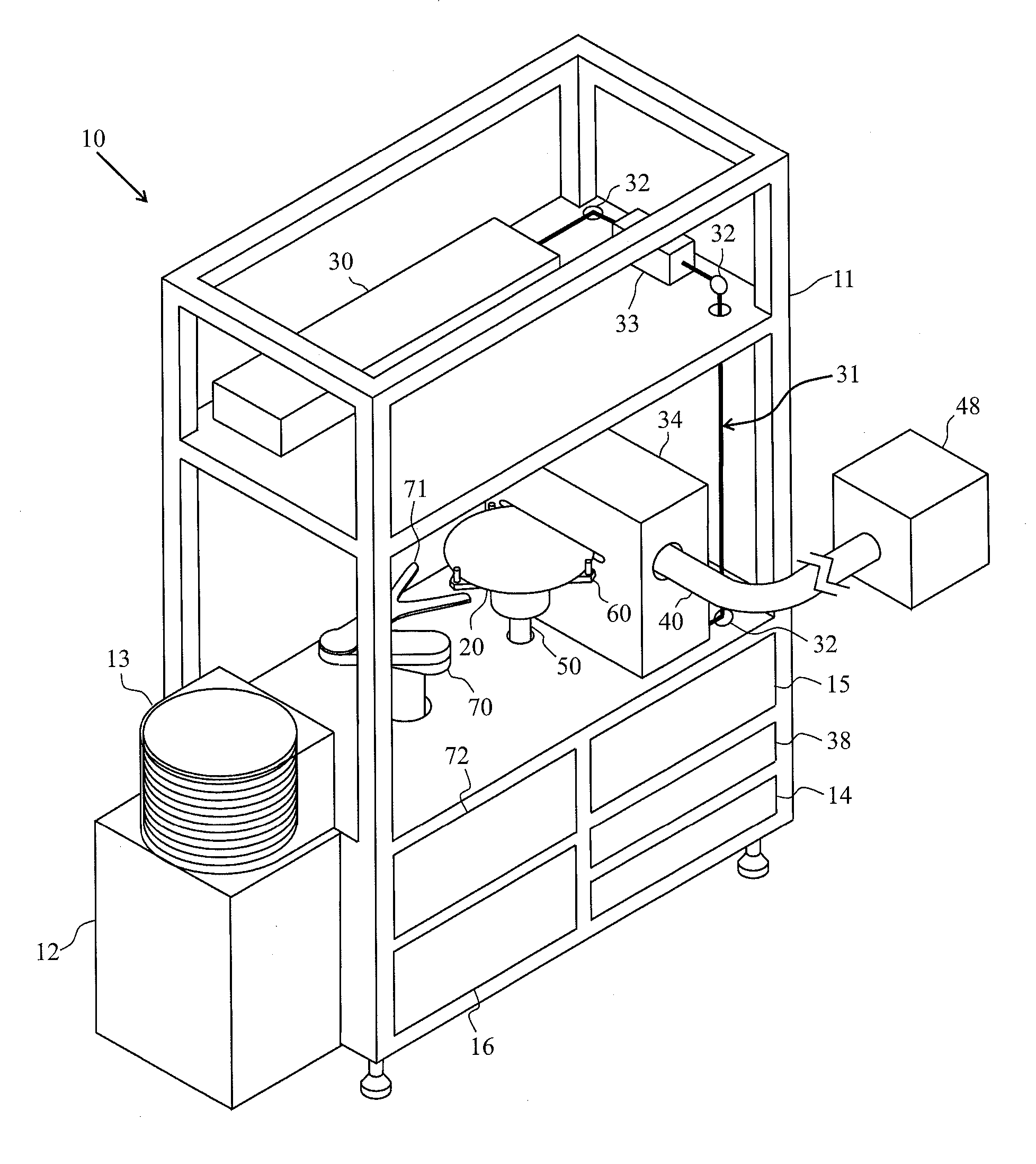
Wafer edge processing in semiconductor manufacturing requires many different types of chemicals and tools, and is therefore complex and costly.
One example of a problem with the prior art relates to a method for dispensing liquid in a solvent-based edge cleaning process, as described in U.S. Pat. No. 5,392,989 and U.S. Patent Application Publication No. 2010 / 0051073 A1.
This problem relates to the inability of the liquid solvent to control the geometry of the cleaned edge.
Solvent-based edge cleaning cannot currently meet this specification due to the inability to effectively control the solvents.
This inability includes solvent splashing onto good die causing yield loss.
Organic solvents, such as ethyl lactate or cellosolve acetate, cause environmental problems, raise safety concerns, and are costly to use.
These chemicals are hazardous to use and require the use of complex and costly equipment, raising environmental problems and safety concerns.
As with the solvent method listed above, it is difficult to effectively control the width of the edge exclusion zone.
This method is specifically used to remove metal films, but due to the non-uniformity of these films at the edge of the wafer, it is difficult to control the etch depth.
This method is also used for removing Teflon-like particles, but is not effective for removing photoresists.
Since multiple pieces of equipment are used, this increases the time to complete the process, reducing throughput.
The exposure step is often not adequate in removal of very thick edge beads; therefore a solvent cleaning process step is required.
This method addresses photoresist edge beads, but there are many other types of more difficult films, such as post-etch polymers, that need to be removed, but cannot be addressed with WEE.
Another example of a problem with the prior art relates to a lithographic masking method, as described in U.S. Patent Application Publication No. 2007 / 0093067 A1 and U.S. Pat. No. 7,745,095 B2.
This method is complex in that at least four individual steps are required to clean the wafer edge.
This method requires multiple pieces of expensive equipment, consumes considerable volumes of solvent and water, and reduces throughput.
Another example of a problem with the prior art relates to a method using reactive plasma, as described in U.S. Pat. No. 7,651,585 B2 and U.S. Patent Application Publication No. 2010 / 0099265 A1.
The width of the gradient adds to the edge exclusion zone, thereby reducing the usable die area.
The complexity of the tool, as well as the vacuum chamber pump time, adds considerable cost and limits throughput.
Another example of a problem with the prior art relates to mechanical methods for cleaning wafer edges as described in U.S. Patent Application Publication No. 2010 / 0190416 A1 and U.S. Patent Application Publication No. 2009 / 0029629 A1.
This method leads to loss of usable die due to particle generation.
Another example of a problem with the prior art relates to the use of frozen carbon dioxide particles to clean wafer edges, as described in U.S. Pat. No. 7,270,136 B2.
The problems with this method are that the equipment used to perform this process is highly complex and expensive, and the impact of the frozen particles can cause damage to the substrate and to otherwise usable die.
Another example of a problem with the prior art relates to applying a flame to the edge of a wafer in the presence of reactive gasses including halogens and ozone, as described in U.S. Patent Application Publication No. 2008 / 0010845 A1.
Nitrogen trifluoride is a highly toxic and expensive gas that is typically used to clean deposition chambers in semiconductor manufacturing.
Further, this method may require pre-heating the wafer to prevent condensation of the by-products onto the wafer, causing die loss.
The apparatus described is very complex since the gas plumbing and safety requirements are extreme for the types of gases proposed for this edge cleaning method.
Lastly, the method cannot remove films from all wafer edges in a single step and is not effective for photoresist removal.
Another example of a problem with the prior art relates to the use of a pressurized stream of a non-solvent medium, which may be a gas, to clean wafer edges, as described in U.S. Patent Application Publication No. 2004 / 0126923 A1.
An expected problem with this method would be the scattering of particles onto the usable areas of the wafer, as well as the surrounding equipment.
Additionally, this patent application claims that the medium must not be a solvent for the material being removed, which severely limits use on a variety of films due to its non-reactive nature.
Finally, another example of a problem with the prior art relates to the method of using an oblique-angled nozzle containing a laser beam combined with inert gas, as described in U.S. Pat. No. 6,874,510 B2.
One problem with this method is that the beam used to clean the wafer edge is inside the gas delivery nozzle, such that the gas cannot be independently directed to prevent material from falling onto the good die toward the center of the wafer.
Such laser reactions create a cloud of debris.
If the gas nozzle is not positioned to remove this cloud away from the center of the wafer, debris will re-deposit onto good die causing yield loss.
This prior art uses a chamber, which further complicates the process of removing the debris, as it becomes confined in the chamber, and can re-deposit onto the wafer as well as build-up on the chamber walls.
Another problem with this prior art method is that the gas used is inert, and therefore does not permit reaction with films on the wafer edges.
Yet another problem with this prior art is that this method shows cleaning only on the top surface.
However, if a source of this type were redirected to the apex, the reaction by-products would be blown onto the good die at the center of the wafer, causing significant die loss.
Still another problem with this prior art is that it requires the laser beam to impinge on the wafer edge at an oblique angle, introducing several problems including beam distortion and focusing issues at the wafer plane.
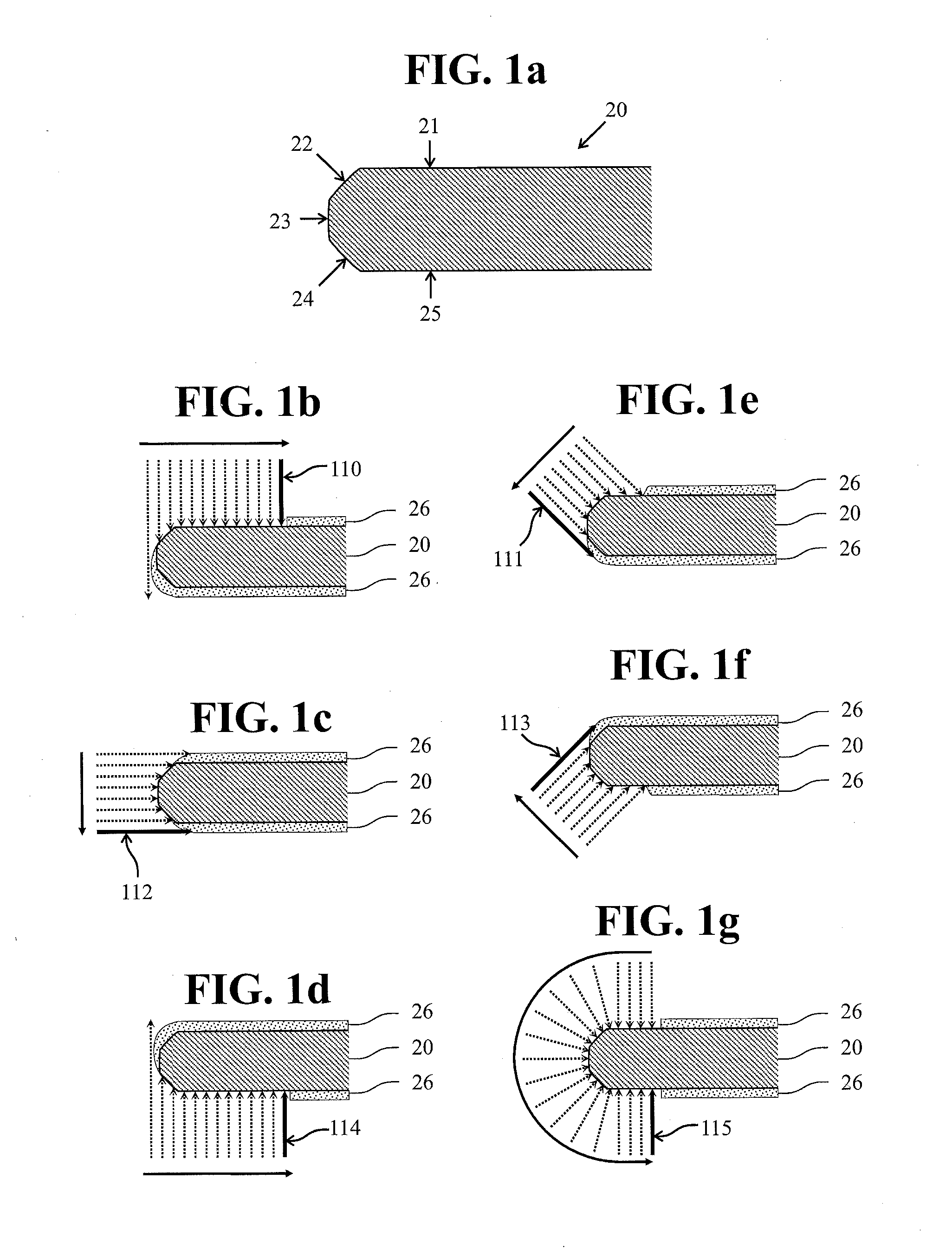
Due to the limitations of current edge cleaning methods, otherwise usable space on the periphery of a wafer is consumed.
Therefore, considerable effort is given to keep the edge cleaning area, called the edge exclusion, to a minimum.
Conventional wet edge bead cleaning methods are unable to control edge exclusion to this level due to the natural movement of liquids on smooth surfaces, such as a highly polished silicon wafer.

Method used


Image

  • Method and apparatus for processing substrate edges
  • Method and apparatus for processing substrate edges
  • Method and apparatus for processing substrate edges

Examples


Embodiment Construction

[0074]A description of example embodiments of the invention follows.

[0075]While the invention as recited in the claims presented elsewhere in this document may be susceptible to embodiment in different forms, there is shown in the drawings, and will be described herein in detail, one or more specific embodiments with the understanding that the present disclosure is to be considered but one exemplification of the principles of the invention, and there is no intent to limit the invention to that as illustrated and described herein. Therefore, any references to “the present invention” and “the disclosure” throughout this document are to be interpreted only as a reference to one particular, non-limiting example embodiment of but one aspect of the many inventions described and disclosed in this document.

[0076]The disclosure describes an apparatus and methods(s) for removing or transforming unwanted films, residues, and particles from the top, top bevel, apex, bottom bevel, and bottom (he...


PUM

PropertyMeasurementUnit
wavelengthaaaaaaaaaa

Abstract

A method and apparatus for processing substrate edges is disclosed that overcomes the limitations of conventional edge processing methods and systems used in semiconductor manufacturing. The edge processing method and apparatus of this invention includes a laser and optical system to direct a beam of radiation onto a rotating substrate supported by a chuck. The optical system accurately and precisely directs the beam to remove or transform organic or inorganic films, film stacks, residues, or particles, in atmosphere, from the top edge, top bevel, apex, bottom bevel, and bottom edge of the substrate in a single process step. An optional gas injector system directs gas onto the substrate edge to aid in the reaction. Reaction by-products are removed by means of an exhaust tube enveloping the reaction site. This invention permits precise control of an edge exclusion width, resulting in an increase in the number of usable die on a wafer. Wafer edge processing with this invention replaces existing methods that use large volumes of purified water and hazardous chemicals including solvents, acids, alkalis, and proprietary strippers.

Description

RELATED APPLICATION(S)[0001]This application is a continuation of U.S. application Ser. No. 12 / 986,914 filed Jan. 7, 2011, which claims the benefit of U.S. Provisional Application No. 61 / 293,325, filed on Jan. 8, 2010 and U.S. Provisional Application No. 61 / 419,602, filed on Dec. 3, 2010. The entire teachings of the above applications are incorporated herein by reference.TECHNICAL FIELD[0002]This patent application generally relates to wafer processing in the manufacture of integrated circuits, and to a method and apparatus for removal of films from semiconductor substrates at various stages of processing. It specifically relates to a laser-based edge processing system for the removal of organic, inorganic, and other semiconductor films from the edges of silicon wafers or other substrates. These films are removed in order to reduce the number of defects generated around the periphery of the wafers that cause loss of good die in integrated circuit manufacturing.BACKGROUND OF THE INVE...

Claims


Application Information

Patent Timeline
Patent Type & Authority Applications(United States)
IPC IPC(8): B23K26/38
CPCB23K26/0621B23K26/063B23K26/0676B23K26/0823B23K26/103B23K2201/40B23K26/16B23K26/362B23K26/4075B23K37/0426B23K37/047B23K26/1405B23K26/361B23K26/142B23K26/0619B23K26/0622B23K26/40B23K2101/40B23K2103/50
Inventor MILLMAN, JR., RONALD P.HARTE, KENNETH J.CHAPLICK, VICTORIA M.ELLIOTT, DAVID J.TARDIF, MURRAY L.DEGENKOLB, EUGENE O.
Owner UVTECH SYST
Why Eureka
Try Eureka