Diode bolometer and method for producing a diode bolometer

a diode bolometer and diode bolometer technology, applied in the direction of pyrometry using electric radation detectors, basic electric elements, electric apparatus, etc., can solve the problems of increasing the demand for miniaturization, inability to take into account devices, and inability to solve long-term problems

Inactive Publication Date: 2011-06-16
FRAUNHOFER GESELLSCHAFT ZUR FOERDERUNG DER ANGEWANDTEN FORSCHUNG EV
View PDF6 Cites 40 Cited by
  • Summary
  • Abstract
  • Description
  • Claims
  • Application Information

AI Technical Summary

Benefits of technology

[0013]According to an embodiment, a bolometer array having pixel elements arranged in columns and rows, each one thereof forming a bolometer, may have: an underlying substrate; a semiconductor membrane per pixel element, having a single-crystalline portion, wherein complementarily doped regions of the single-crystalline portion form a diode and a p-n junction extends between same along a column direction, pixel elements neighboring in the column direction exhibiting equal doping profiles; and a first and a second spacer per pixel element so as to keep the semiconductor membrane at a predetermined distance from th

Problems solved by technology

When the alteration in the resistance of the material induced by the change in temperature is smaller than the noise of the electrical parameters, it will no longer be resolved.
However, this approach is of the decisive disadvantage that the increasing demand for miniaturization and, thus, making the devices cheaper, cannot be taken into account.
This represents a serious problem in that the integrative read-out circuits conventionally used (low pass), for example, are not suitable for suppressing predominant low-frequency noise portions.
However, integrating thermally insulating diodes in a CMOS process is complicated.
The approach used at first of manufacturing insulated diodes directly in the CMOS wafer by means of suitable under-etchings is of dis

Method used


Image

  • Diode bolometer and method for producing a diode bolometer
  • Diode bolometer and method for producing a diode bolometer
  • Diode bolometer and method for producing a diode bolometer

Examples


Embodiment Construction

[0045]Before discussing the present invention in greater detail below referring to the drawings, it is pointed out that same elements in the figures are provided with same or similar reference numerals and that a repeated description of these elements is omitted.

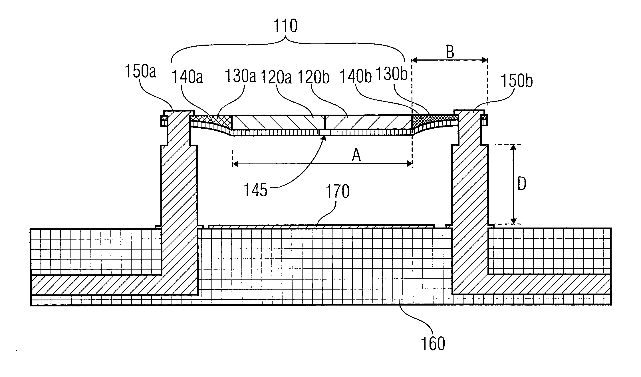
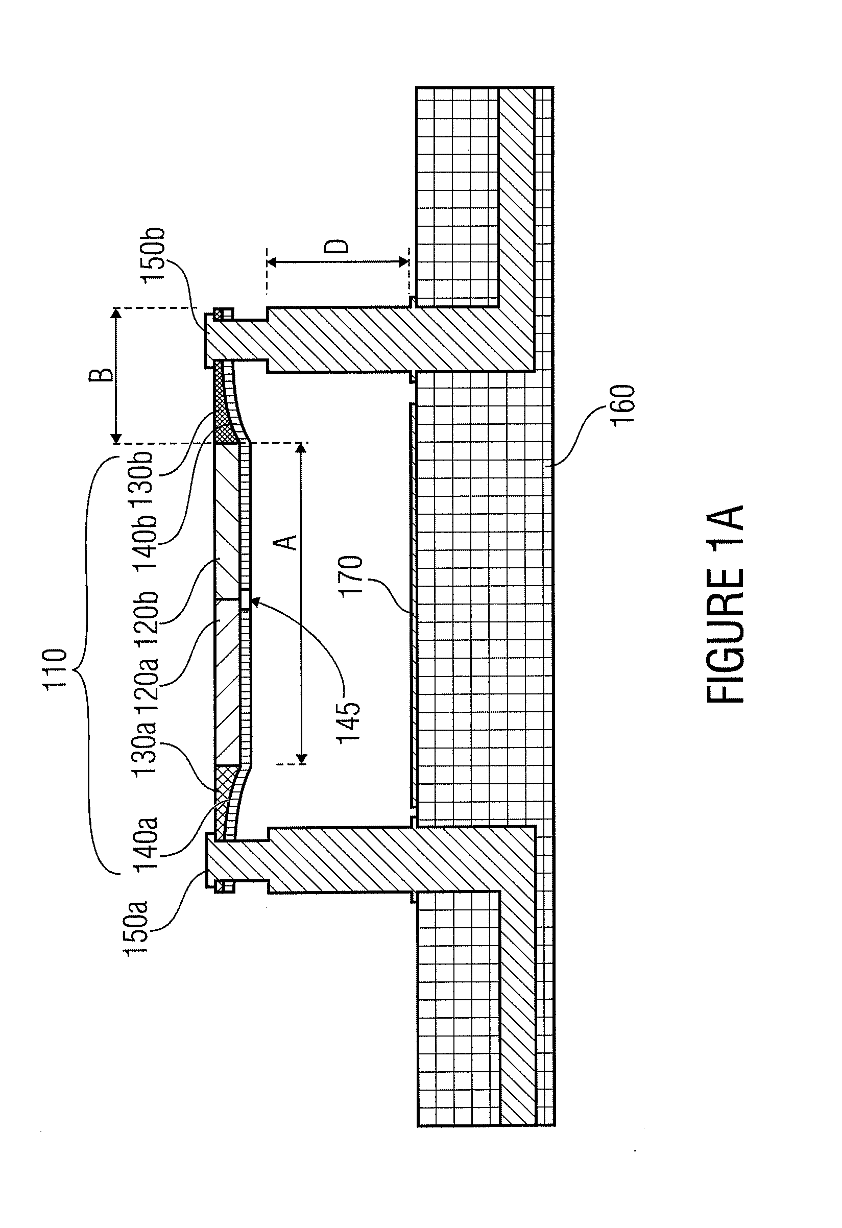
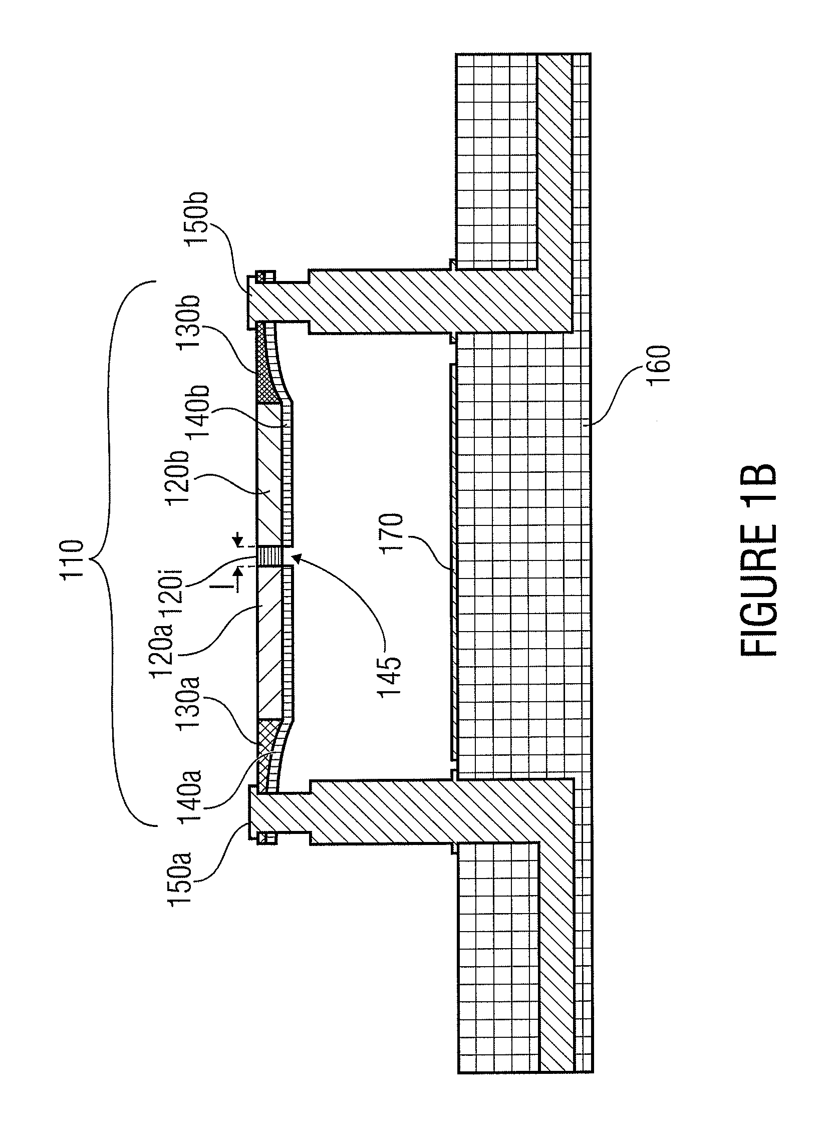
[0046]FIG. 1a shows a cross-sectional view of a bolometer in accordance with an embodiment of the present invention, the bolometer comprising a semiconductor membrane 110 which is kept at a certain distance D from an underlying substrate 160 by two spacers 150a, b. The semiconductor membrane 110 comprises a single-crystalline portion 120, complementarily doped regions 120a, b of the single-crystalline portion 120 forming a diode. Additionally, the semiconductor membrane 110 comprises a first amorphized region 130a which is in connection with the first spacer 150a, and a second amorphized region 130b which is in contact with the second spacer 150b. A conductive layer 140 is formed on that side of the membrane 110 facing the u...


PUM


Abstract

A bolometer has a semiconductor membrane having a single-crystalline portion, and spacers so as to keep the semiconductor membrane at a predetermined distance from an underlying substrate. The complementarily doped regions of the single-crystalline portion form a diode and the predetermined distance corresponds to a fourth of an infrared wavelength.

Description

CROSS-REFERENCE TO RELATED APPLICATIONS[0001]This application is a continuation of copending International Application No. PCT / EP2008 / 004589, filed Jun. 9, 2008, which is incorporated herein by reference in its entirety.BACKGROUND OF THE INVENTION[0002]The present invention relates to a diode bolometer and to a method for producing a diode bolometer and, in particular, to a diode bolometer exhibiting reduced thermal coupling and to a method for producing of high alignment tolerance.[0003]Detecting infrared radiation is increasing in importance in many different fields. For the automobile industry, this importance is achieving an increase in the security of, for example, pedestrians who can be made visible using infrared sensors also in dark environments. When coupling an automatic brake system to sensor technology, accidents can be avoided or at least the consequences thereof be reduced. Further applications of infrared sensors exemplarily include examining technical apparatuses (su...

Claims


Application Information

Patent Timeline
IPC IPC(8): H01L31/0232H01L31/18H01L31/09
CPCH01L21/2007G01J5/20
Inventor KROPELNICKI, PIOTRRUSS, MARCOVOGT, HOLGER
Owner FRAUNHOFER GESELLSCHAFT ZUR FOERDERUNG DER ANGEWANDTEN FORSCHUNG EV
Why Eureka
Try Eureka