Group iii nitride semiconductor substrate and manufacturing method of the same

a technology of nitride and semiconductor substrate, which is applied in the direction of crystal growth process, semiconductor laser, polycrystalline material growth, etc., can solve the problem of large difference in lattice constant between sapphire and gan crystal, ultra-high density of crystal defects in grown gan, and sometimes a barrier between crystal defects, etc. problem, to achieve the effect of little disturbance of flatness

Inactive Publication Date: 2011-06-23
HITACHI METALS LTD
View PDF8 Cites 5 Cited by
  • Summary
  • Abstract
  • Description
  • Claims
  • Application Information

AI Technical Summary

Benefits of technology

[0011]An object of the present invention is to provide the group III nitride semiconductor substrate capable of obtaining a flat cleavage plane with little disturbance of flatness such as a macro-step, and a manufacturing method of the same.

Problems solved by technology

However, even in this method, difference of the lattice constant between the sapphire and the GaN crystal is still greatly problematic, and the grown GaN has ultra-high density of crystal defects.
Such crystal defects are sometimes a barrier in manufacturing GaN-based LDs and high luminance LEDs.
In a case of GaN, it is difficult to grow a large sized ingot from melt like Si and GaAs.
However, in an actual cleavage plane, disturbance of flatness such as a macro-step (difference-in-level) is generated due to various factors, thus causing decrease in yield rate of LDs. FIG. 5 shows a differential interference contrast image obtained by observing the cleavage plane formed by cleaving a conventional GaN substrate manufactured by HVPE, using a differential interference microscope (“BX11” by OLYMPUS Corporation).

Method used


Image

  • Group iii nitride semiconductor substrate and manufacturing method of the same
  • Group iii nitride semiconductor substrate and manufacturing method of the same
  • Group iii nitride semiconductor substrate and manufacturing method of the same

Examples


example 1

[0062]In example 1, the GaN substrate was manufactured, having a tensile stress part in the outer peripheral part of the substrate. The manufacturing step of the GaN substrate and the cleavage of the obtained GaN substrate according to the example 1 will be described by using FIG. 1.

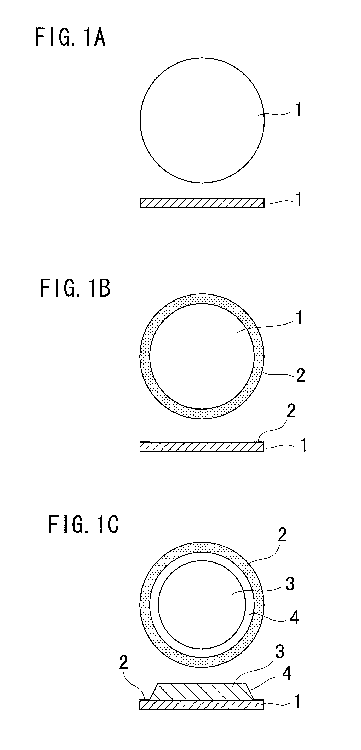
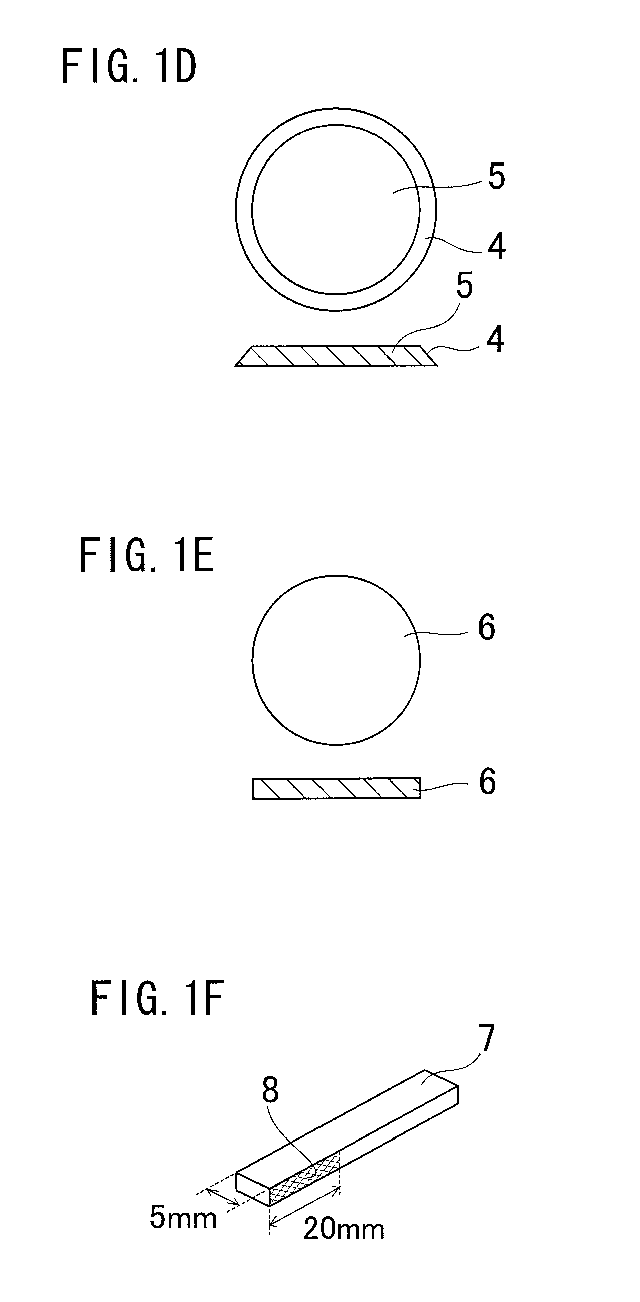
[0063]First, a disc-shaped GaN freestanding substrate (seed crystal substrate) 1 having diameter of 60 mm and thickness of 400 μm was prepared, with c-plane (Ga plane) as the main surface (growth plane) (FIG. 1A). It was confirmed by the photoelastic measurement, that a stress distribution of the seed crystal substrate 1 was approximately uniform. Note that in each figure of FIG. 1A to FIG. 1E, an upper part is a plan view, a lower part is a sectional view, and FIG. 1F is a perspective view of the GaN substrate cleaved in a state of bars.

[0064]Next, an annular high purity carbon mask 2 having a circular opening with diameter of 55 mm was overlapped on the seed crystal substrate 1 (FIG. 1B), which was the...

example 2

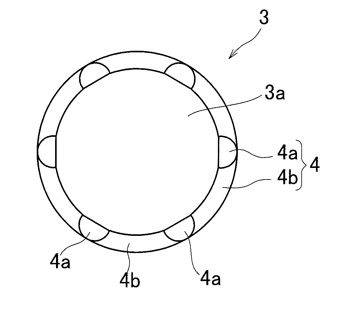
[0076]First, the GaN substrate 6 was manufactured in the same way as the example 1. However, an oxygen supply amount during HVPE growth was adjusted, so that the oxygen concentration of the inclined growth part of the GaN layer 3 was 5×1020 cm−3. Further, a grinding amount of the outer periphery of the GaN substrate 5 having the inclined growth part was increased, so that the diameter of the GaN substrate 6 was 45 mm. It was confirmed by the photoelastic measurement, that the outer peripheral tensile stress of 80 MPa was remained on the GaN substrate 6 of the example 2, after outer peripheral grinding was applied thereto.

[0077]The epitaxial layers with LD structure similar to the example 1 were grown on the GaN substrate 6 by the MOVPE method, then rear surface grinding was applied thereto to process the thickness to 200 μm, and thereafter the GaN substrate was cleaved to examine the density of macro-steps in the cleavage plane. Then, an extremely excellent value of 0.08 / mm was obta...

example 3

[0081]In the example 3, the GaN freestanding substrate (seed crystal substrate) 1 with diameter of 6 inches (152.4 mm) and an annular high purity carbon mask 2 having a circular opening with diameter of 147.4 mm were used to carry out the growth of the GaN layer 3 of 1200 μm. In addition, the GaN substrate 5 with thickness of 1000 μm, with a bottom part having diameter of 147.4 mm, and having the inclined growth part was obtained by the manufacturing method similar to the example 1.

[0082]Note that the seed crystal substrate 1 with diameter of 6 inches is the substrate obtained by forming the GaN thin film and vapor-depositing a Ti layer on the sapphire substrate having diameter of 6 inches, and by applying heat treatment thereto, forming a void structure in the GaN thin film, then making GaN grown thick thereon by the HVPE method, and separating the sapphire substrate from the void structure part.

[0083]Even in the GaN substrate 5 of the example 3, in the same way as the example 1, i...


PUM

PropertyMeasurementUnit
thicknessaaaaaaaaaa
thicknessaaaaaaaaaa
diameteraaaaaaaaaa

Abstract

A Group III nitride semiconductor substrate is provided, with diameter of 25 mm or more and thickness of 250 μm or more, wherein in at least an outer edge side part of an outer edge part within 5 mm from an outer edge of the group III nitride semiconductor substrate, stress within a main surface of the group III nitride semiconductor substrate works as a tensile stress, with the tensile stress becoming relatively greater compared to that of a center side part from the outer edge side part of the group III nitride semiconductor substrate.

Description

BACKGROUND[0001]1. Technical Field[0002]The present invention relates to a group III nitride semiconductor substrate and a manufacturing method of the same, and particularly relates to the group III nitride semiconductor substrate improved in cleavage characteristics and the manufacturing method of the same.[0003]2. Description of Related Art[0004]Group III nitride semiconductors such as gallium nitride (GaN), indium gallium nitride (InGaN), and aluminium gallium nitride (AlGaN) attract attention as materials of light emitting diodes (LEDs) of blue color and laser diodes (LDs) of blue color. Further, by taking advantage of the characteristics of the group III nitride semiconductor such as having excellent heat resistance property and environmental resistance property, development of application to electronic devices has been started.[0005]A substrate for GaN growth in wide practical use at present is sapphire, and a method of epitaxially-growing GaN by metal-organic vapor phase epit...

Claims


Application Information

Patent Timeline
Patent Type & Authority Applications(United States)
IPC IPC(8): H01L29/20H01L21/20
CPCB82Y20/00C30B25/04C30B29/403H01L21/02389H01S5/34333H01L21/0262H01S5/0042H01S5/0202H01L21/0254
Inventor OSHIMA, YUICHI
Owner HITACHI METALS LTD
Why Eureka
Try Eureka