High read speed electronic memory with serial array transistors

Active Publication Date: 2011-06-23
INFINEON TECH LLC
View PDF12 Cites 5 Cited by
  • Summary
  • Abstract
  • Description
  • Claims
  • Application Information

AI Technical Summary

Benefits of technology

The subject disclosure provides a serial semiconductor memory architecture achieving fast program, erase and read times as compared with conventional serial semiconductor memory architectures. The architecture comprises a serial array of memory transistors coupled to a metal bitline of an electronic memory device at one end of the array, and a gate of a pass transistor at an opposite end of the array. In some aspects of the subject disclosure, the pass transistor has low capacitance relative to the metal bitline or relative to the serial array of memory transistors.
A second metal bitline is then coupled to the drain of this pass transistor, while ground is coupled to the source of this pass transistor. Current flow through the second bitline is modulated by the potential on the gate of the pass transistor. Coupled to the second bitline is a sensing circuit which can be utilized to detect current flow, which is indicative of a state of a memory cell of the serial array. Accordingly, a serial array of memory transistors connected to a first metal bitline can be sensed from a second metal bitline of the memory device. Further, because the pass transistor has relatively small capacitance, a relatively small amount of current through the serial array is sufficient to charge or discharge a gate node of the pass transistor, enabling/disabling current flow at the second metal bitline. Accordingly, sensing a program or erase state of a m

Problems solved by technology

One major limiting factor for speed and sophistication of electronic devices and complexity of device software is the physical capabilities of digital me

Method used


Image

  • High read speed electronic memory with serial array transistors
  • High read speed electronic memory with serial array transistors
  • High read speed electronic memory with serial array transistors

Examples


Example

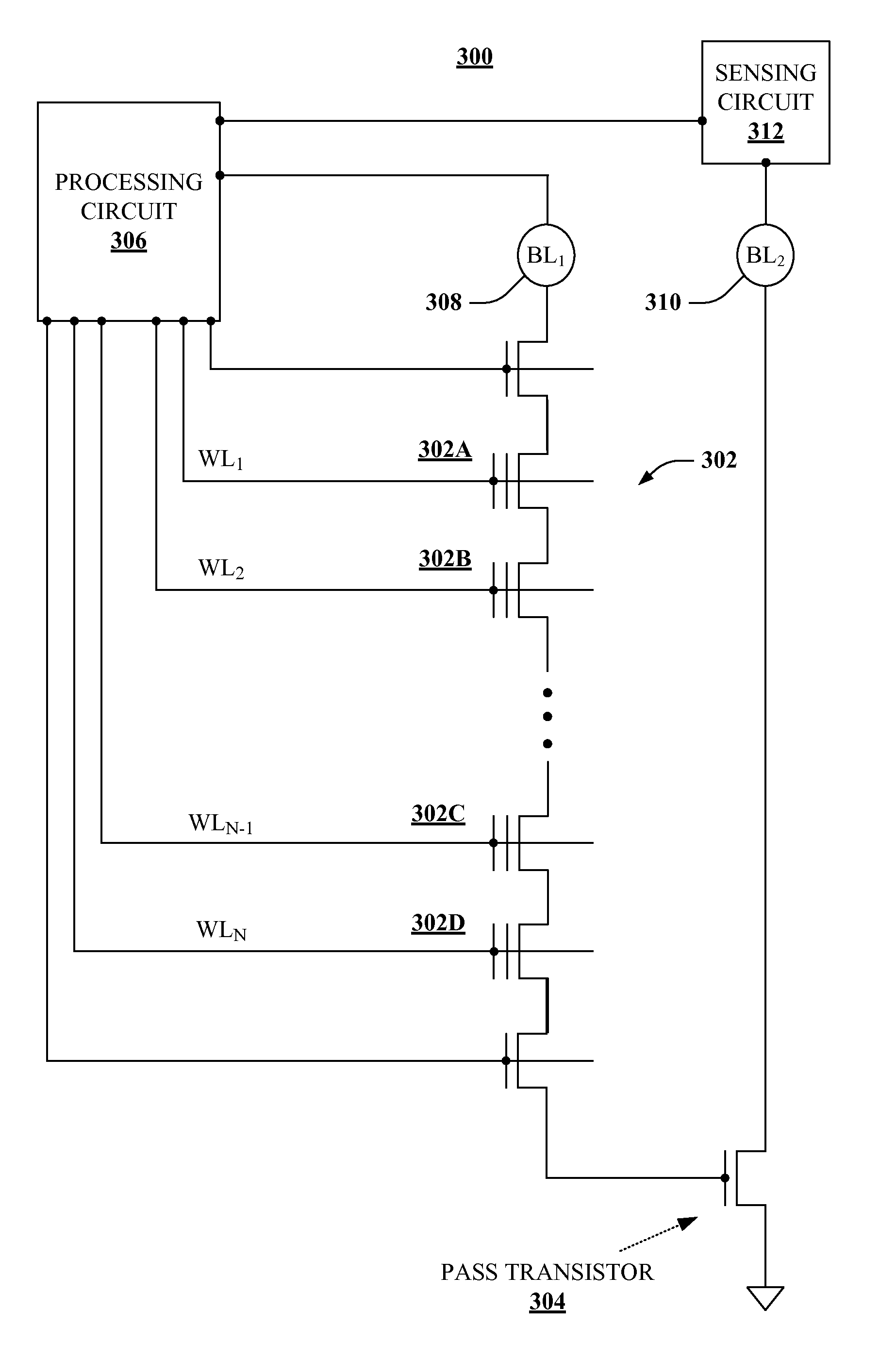
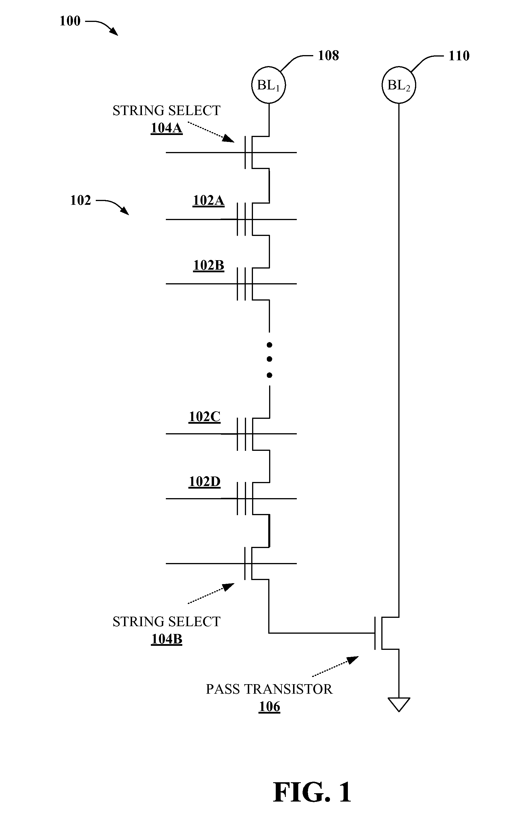
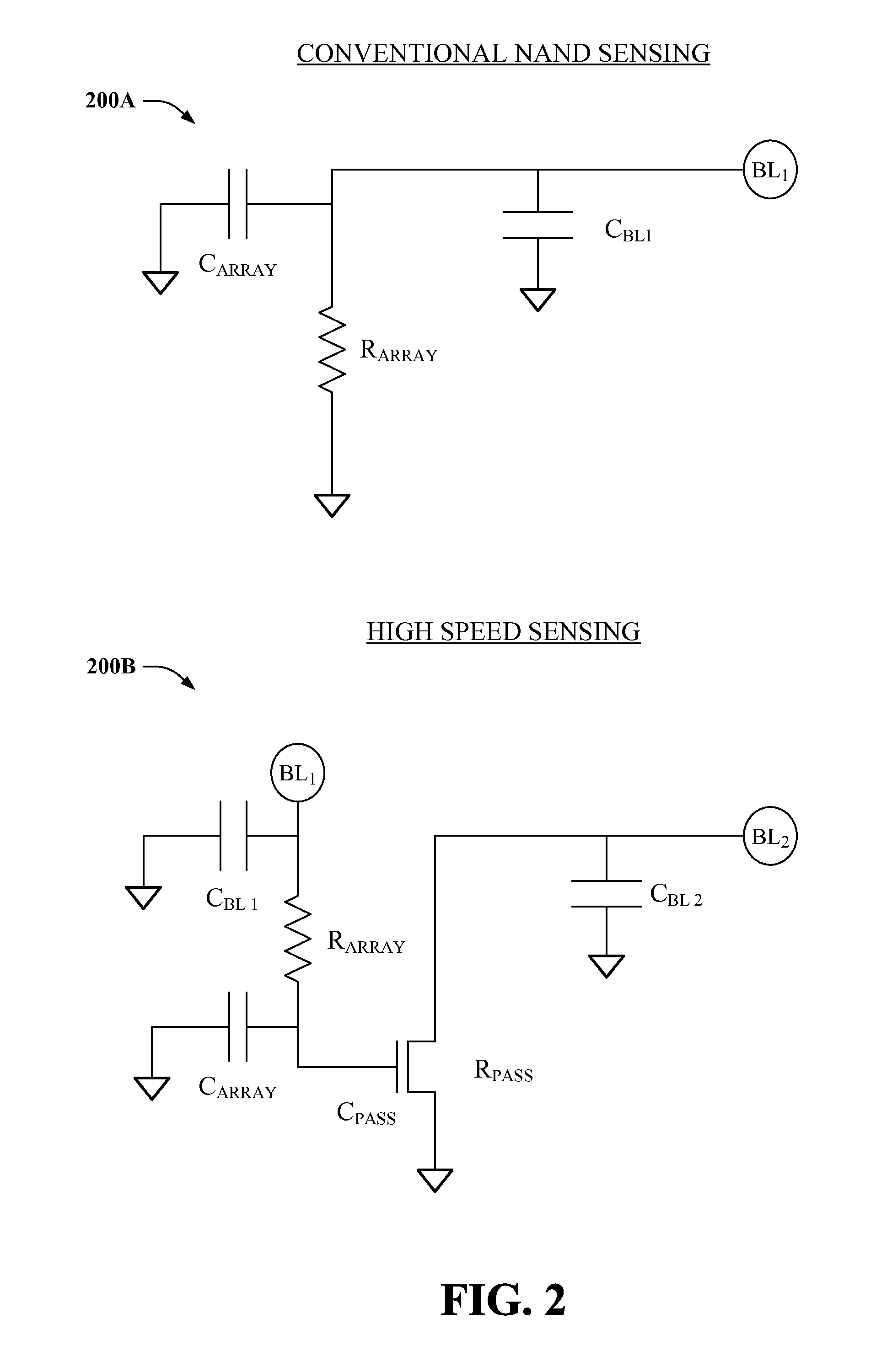
The disclosed subject matter is described with reference to the drawings, wherein like reference numerals are used to refer to like elements throughout the description. In the following description, for purposes of explanation, numerous specific details are set forth in order to provide a thorough understanding of the subject innovation. It may be evident, however, that the disclosed subject matter may be practiced without these specific details. In other instances, well-known structures and devices are shown in block diagram or schematic form in order to facilitate describing the subject innovation.

As utilized herein, terms “component,”“system,”“architecture” and the like are intended to refer to a computer or electronic-related entity, either hardware, a combination of hardware and software, software (e.g., in execution), or firmware. For example, a component can be one or more semiconductor storage cells, a processor, a process running on the processor, an object, an executable, ...


PUM


Abstract

Providing a serial array semiconductor architecture achieving fast program, erase and read times is disclosed herein. By way of example, a memory architecture can comprise a serial array of semiconductors coupled to a metal bitline of an electronic memory device at one end of the array, and a gate of a pass transistor at an opposite end of the array. Furthermore, a second metal bitline is coupled to a drain of the pass transistor. A sensing circuit that measures current or voltage at the second metal bitline, which is modulated by a gate potential of the pass transistor, can determine a state of transistors of the serial array. Because of low capacitance of the pass transistor, the serial array can charge or discharge the gate of the pass transistor quickly, resulting in read times that are significantly reduced as compared with conventional serial semiconductor array devices.

Description

BACKGROUNDMemory devices have a wide range of uses in modern electronics and electronic devices. In general, various types of electronic memory exist, including hard disc memory, floppy disc memory, magnetic tape memory, optical disk memory, and so on. One of the more innovative and diversified types of memory is semiconductor memory.One type of semiconductor memory commonly used for modern electronics is nonvolatile Flash memory. Flash memory comprises arrays of semiconductor devices that can be utilized to store, erase and re-store digital information. Compared to other types of electronic memory, Flash memory is fast both in terms of programming and erasing, as well as reading data, has good data retention characteristics, and is highly cost effective. Accordingly, Flash memory is utilized for data storage in an ever-increasing number of electronic devices and applications, including computers, cell phones, smart-phones, digital cameras and camcorders, game stations, and so forth...

Claims


Application Information

Patent Timeline
IPC IPC(8): G11C5/06G11C7/06H01L21/336
CPCG11C16/26G11C16/24
Inventor FASTOW, RICHARDNAZARIAN, HAGOP
Owner INFINEON TECH LLC
Why Eureka
Try Eureka