Pecvd multi-step processing with continuous plasma

Inactive Publication Date: 2011-06-23
APPLIED MATERIALS INC
View PDF4 Cites 114 Cited by
  • Summary
  • Abstract
  • Description
  • Claims
  • Application Information

AI Technical Summary

Benefits of technology

[0013]In another embodiment, a method for processing a substrate disposed within a processing chamber includes providing a first gas mixture by flowing one or more precursor gases and an inert gas to the chamber, applying an electric field to the gas mixture and heating the gas mixture to decompose the one or more precursor gases in the gas mixture to generate a plasma, depositing the first material on the substrate until a desired thickness of the first material is achieved, terminating at least one gas flow of the one or more precursor gases in the first gas mixture while flowing only the inert gas and maintaining the plasma, stabilizing a process condition for a second material within the processing chamber, providing a second gas mixture by flowing one or more precursor gases to the same processing chamber, wherein the first gas mixture and the second ga

Problems solved by technology

This uneven topology can cause reflection and refraction of the incident radiant energy, resulting in exposure of some of the photoresist beneath the opaque portions of the mask.
As a result, this uneven surface topology can alter the patterns transferred by the photoresist layer, thereby altering critical dimensions of the structures fabricated.
However, this conventional method allows for particles to contaminate the substrate at the end of every deposition since no repulsive force (e.g., van der waals force) is presented between the substrate and particles when plasma is extinguished, causing unwanted particles to adsorb or fall on the substrate during th

Method used


Image

  • Pecvd multi-step processing with continuous plasma
  • Pecvd multi-step processing with continuous plasma
  • Pecvd multi-step processing with continuous plasma

Examples


Embodiment Construction

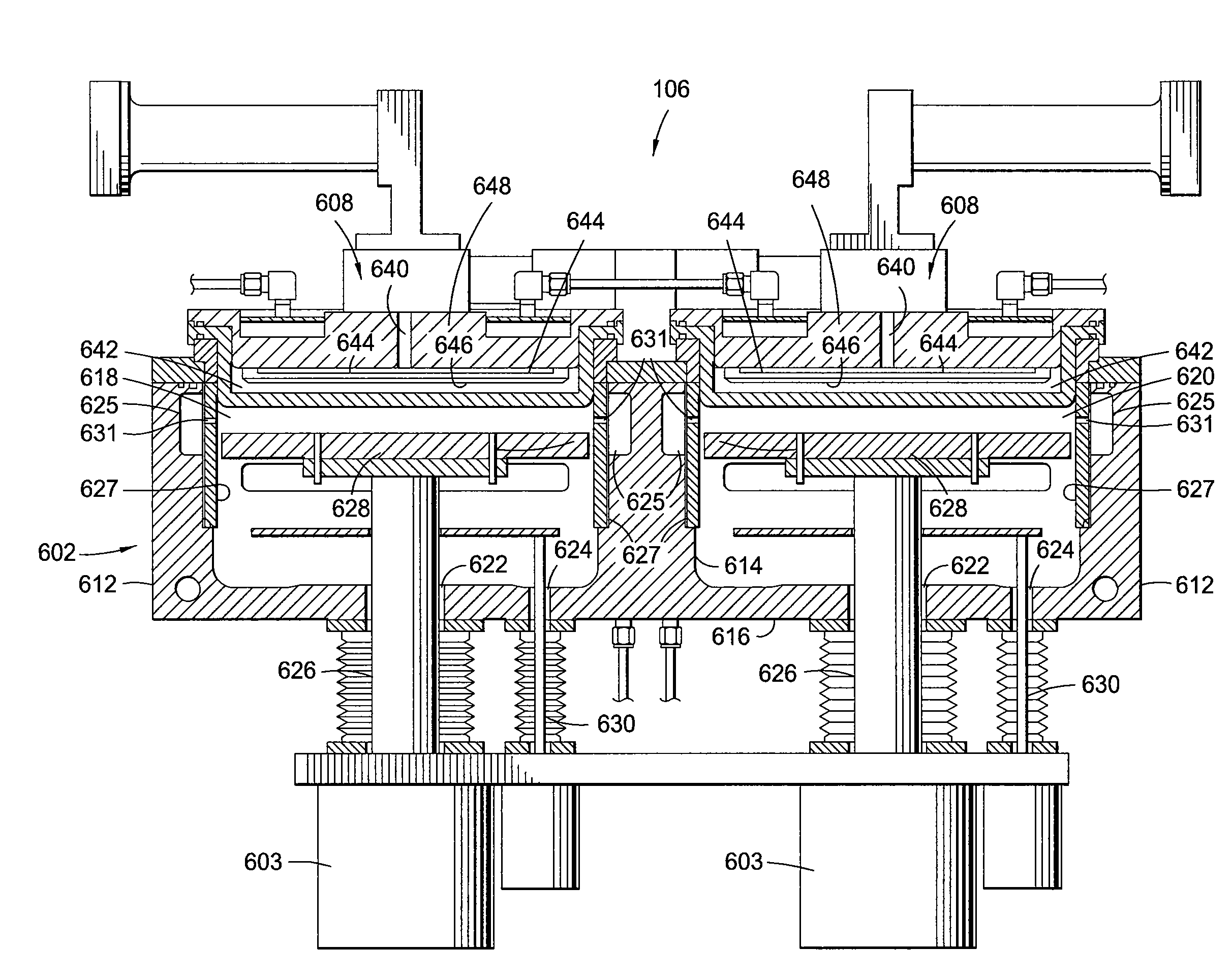
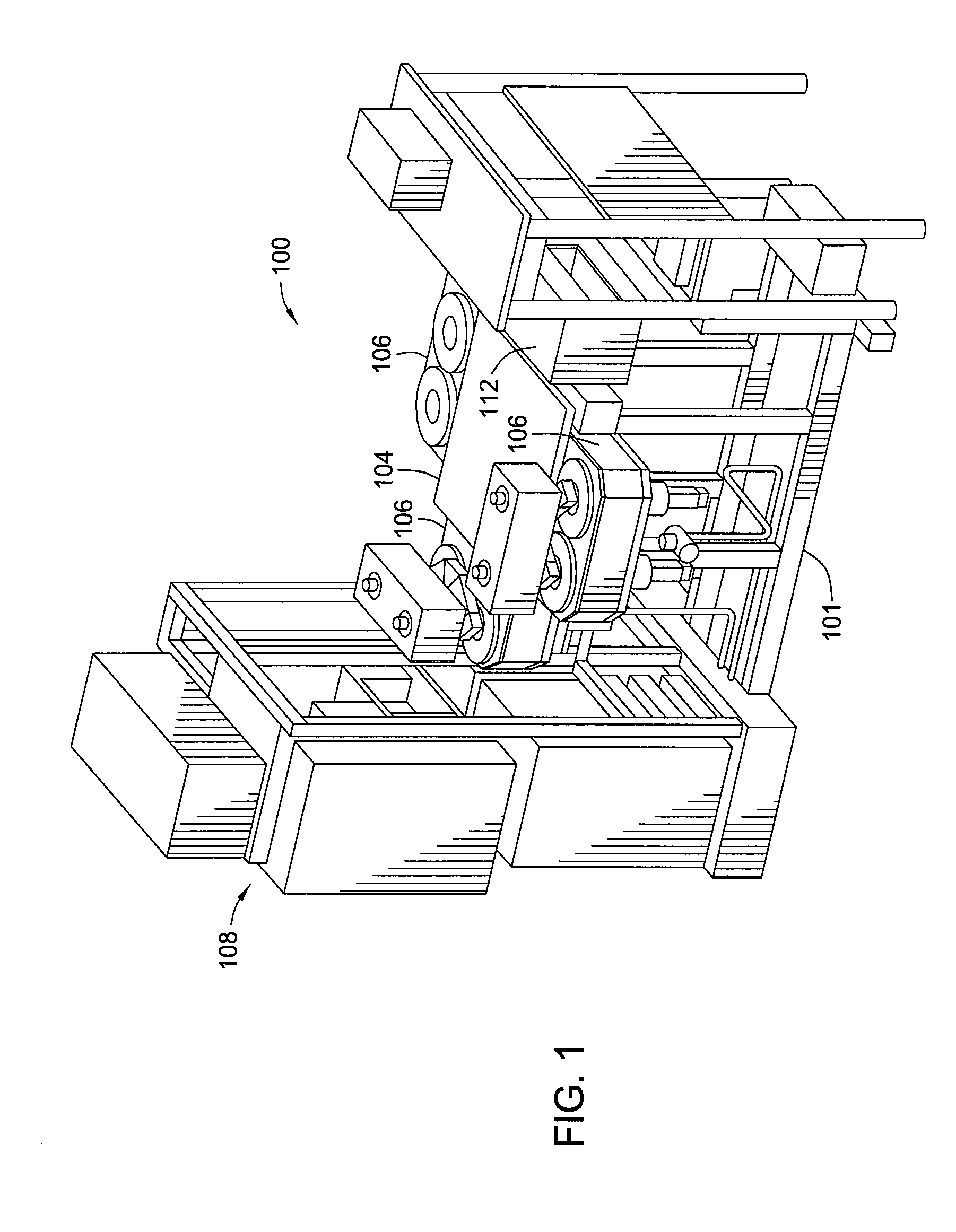
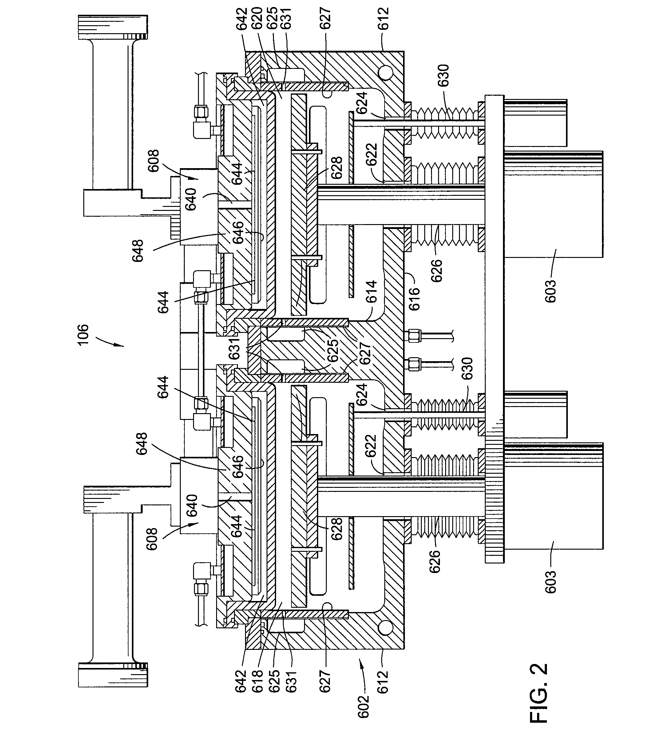
[0020]The present invention provides a method for reducing defects formed during multi-layer deposition within a processing chamber. Films that can benefit from this process include dielectric materials such as silicon oxide, silicon oxynitride, or silicon nitride films that may be used as a dielectric antireflective coating (DARC). In one embodiment, the defect control is realized by maintaining a continuous plasma between each deposition step such that any particles formed during the previous deposition or flaking off from the surfaces of the processing chamber are suspended in the plasma, preventing unwanted particles from falling on the substrate. The unwanted particles will remain suspending in the plasma until the final layer deposition is finished and be removed by a purging and pumping steps to minimize chances of contaminating the substrate during the entire deposition process. In another embodiment, an inert gas is continuously flowing into the processing chamber to mainta...


PUM

PropertyMeasurementUnit
Poweraaaaaaaaaa
Poweraaaaaaaaaa
Frequencyaaaaaaaaaa

Abstract

Embodiments of the present invention provide methods for reducing defects during multi-layer deposition. In one embodiment, the method includes exposing the substrate to a first gas mixture and an inert gas in the presence of a plasma to deposit a first material layer on the substrate, terminating the first gas mixture when a desired thickness of the first material is achieved while still maintaining the plasma and flowing the inert gas, and exposing the substrate to the inert gas and a second gas mixture that are compatible with the first gas mixture in the presence of the plasma to deposit a second material layer over the first material layer in the same processing chamber, wherein the first material layer and the second material layer are different from each other.

Description

CROSS-REFERENCE TO RELATED APPLICATIONS[0001]This application claims benefit of U.S. provisional patent application Ser. No. 61 / 289,300, filed Dec. 22, 2009, which is incorporated by reference herein.BACKGROUND OF THE INVENTION[0002]1. Field of the Invention[0003]Embodiments of the present invention generally relate to the fabrication of integrated circuits. In particular, embodiments of the present invention relate to method for reducing defects during multi-layer deposition within a processing chamber.[0004]2. Description of the Related Art[0005]In the manufacture of integrated circuits, chemical vapor deposition processes are often used for deposition or etching of various material layers. Conventional thermal CVD processes supply reactive compounds to the substrate surface where heat-induced chemical reactions take place to produce a desired layer. Plasma enhanced chemical vapor deposition (PECVD) processes employ a power source (e.g., radio frequency (RF) power or microwave pow...

Claims


Application Information

Patent Timeline
IPC IPC(8): H05H1/24
CPCC23C16/45523C23C16/4401H01L21/02274H01L21/0228H01L21/02315
Inventor SEAMONS, MARTIN JAYTANG, SUM-YEE BETTYLIN, MICHAEL H.REILLY, PATRICKRATHI, SUDHA
Owner APPLIED MATERIALS INC
Why Eureka
Try Eureka