Orthogonal Procesing of Organic Materials Used in Electronic and Electrical Devices

US20110159252A1Active Publication Date: 2011-06-30CORNELL UNIVERSITY

Image

  • Orthogonal Procesing of Organic Materials Used in Electronic and Electrical Devices
  • Orthogonal Procesing of Organic Materials Used in Electronic and Electrical Devices
  • Orthogonal Procesing of Organic Materials Used in Electronic and Electrical Devices

Examples


Embodiment Construction

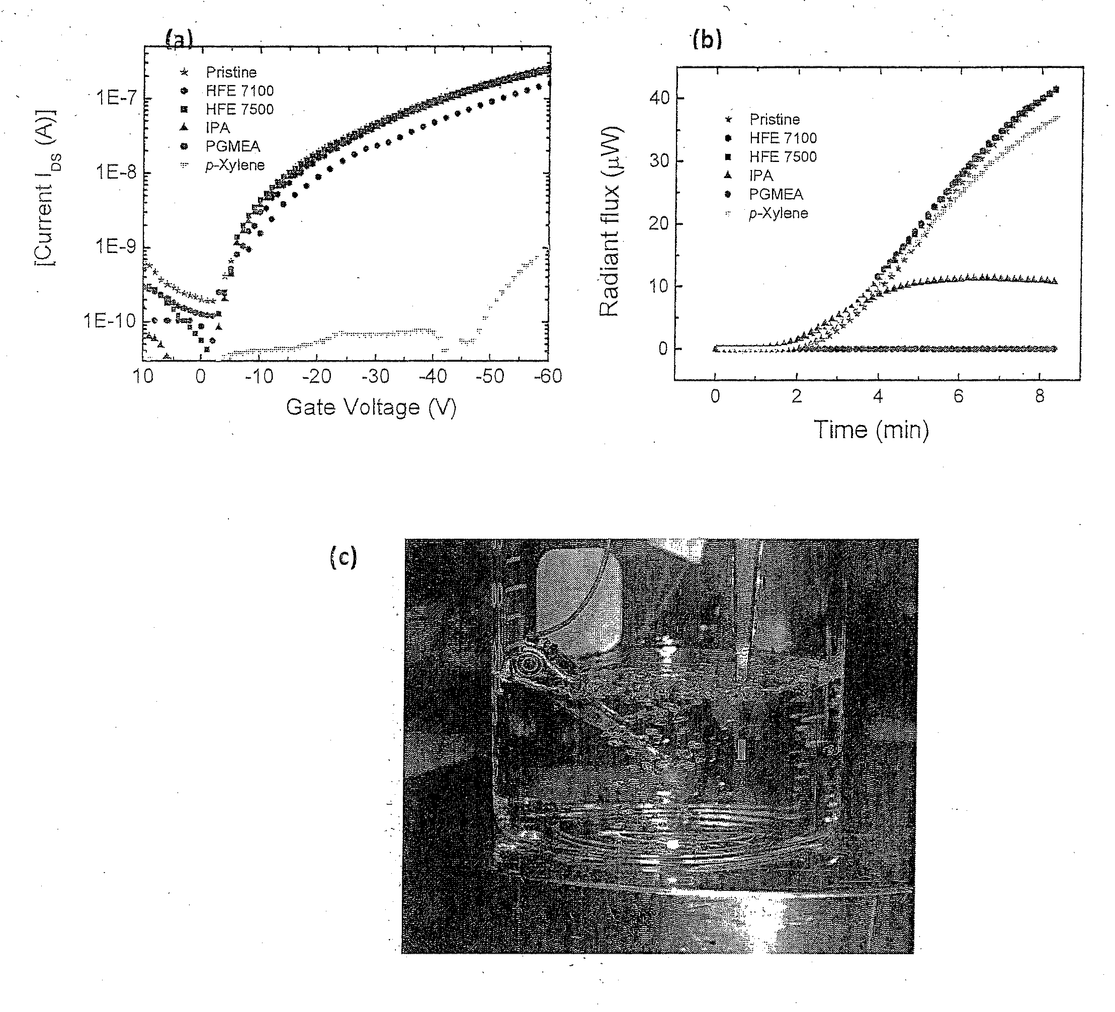
[0059]The term chemical processing as used herein shall mean any chemical treatment such as cleaning, depositing a second layer from solution to form multilayer devices, and depositing / developing resist layers for photolithographic patterning.

[0060]Fluorous Solvents

[0061]Fluorous solvents are perfluorinated or highly fluorinated liquids, which are typically immiscible with organic solvents and water. Among those solvents, segregated hydrofluoroethers (HFEs) are well known to be highly environmentally friendly, “green” solvents. HFEs are non-flammable, have zero ozone-depletion potential, low global warming potential and show very low toxicity to humans. HFEs were introduced to industry in 1994 as third generation hydrofluorocarbon liquids to be used as replacement of chlorofluorocarbons and hydrochlorofluorocarbon refrigerants. HFEs have also been demonstrated as environmental friendly cleaning solvents for electronics. Nevertheless, the use of HFEs in the processing of organic elec...


PUM

PropertyMeasurementUnit
Fractionaaaaaaaaaa
Fractionaaaaaaaaaa
Fractionaaaaaaaaaa

Abstract

An orthogonal process for photolithographic patterning organic structures is disclosed. The disclosed process utilizes fluorinated solvents or supercritical CO2 as the solvent so that the performance of the organic conductors and semiconductors would not be adversely affected by other aggressive solvent. One disclosed method may also utilize a fluorinated photoresist together with the HFE solvent, but other fluorinated solvents can be used. In one embodiment, the fluorinated photoresist is a resorcinarene, but various fluorinated polymer photoresists and fluorinated molecular glass photoresists can be used as well. For example, a copolymer perfluorodecyl methacrylate (FDMA) and 2-nitrobenzyl methacrylate (NBMA) is a suitable orthogonal fluorinated photoresist for use with fluorinated solvents and supercritical carbon dioxide in a photolithography process. The combination of the fluorinated photoresist and the fluorinated solvent provides a robust, orthogonal process that is yet to be achieved by methods or devices known in the art.

Description

BACKGROUND[0001]1. Technical Field[0002]An orthogonal process for patterning organic structures is disclosed which utilizes a fluorinated solvent or supercritical CO2 as a solvent for organic materials. The disclosed process may also utilize a fluorinated photoresist in combination with a fluorinated solvent. The fluorinated photoresist may be a resorcinarene, a copolymer of perfluorodecyl methacrylate and 2-nitrobenzyl methacrylate, derivatives thereof or other polymer photoresist or molecular glass photoresists having sufficient fluorine content. The fluorinated photoresist and fluorinated solvent are used to make patterns of various organic structures used in electronic (semiconductor) and electrical devices. For example, the materials and techniques disclosed herein may be applied to the patterning of acidic poly(3,4-ethylenedioxythiophene):poly(styrenesulfonate) (PEDOT:PSS), a widely used organic material for which no other straightforward lithographic patterning method exists....

Claims


Application Information

Patent Timeline
30 Jun 2011
Publication
US20110159252A1
IPC
B32B3/10; C07C43/23; C08F220/22; C08L33/16; G03F7/20; G03F7/004
CPC
G03F7/0046; G03F7/0392; G03F7/325; Y10T428/24802; H01L51/0018; Y02E10/549; G03F7/40; H10K71/233
Inventors
OBER, CHRISTOPHER K.; MALLIARAS, GEORGE