Method for manufacturing separated micromechanical components situated on a silicon substrate and components manufactured therefrom

a micromechanical and silicon substrate technology, applied in the direction of fluid pressure measurement, semiconductor electrostatic transducers, instruments, etc., can solve the problems of complex sawing using liquid media, high risk of components, and multiple or even multiple laser scans, so as to reduce processing time and processing costs, reduce the cutting depth of the laser process, and reduce the effect of amorphization

Active Publication Date: 2011-07-07
ROBERT BOSCH GMBH
View PDF8 Cites 8 Cited by
  • Summary
  • Abstract
  • Description
  • Claims
  • Application Information

AI Technical Summary

Benefits of technology

[0026]As a result, the separation trenches are also etched less deeply than the cavities. In the case of the known and previously characterized RIE lag effect, it may also be pre-established by the selection of the trench width relative to the cavity width how deep each of the separation trenches is etched in the silicon during the simultaneous application of the cavities. The depth of the separation trenches may be set in such a way that after the etching step the silicon substrate is still stable and may be handled without risk of fracture in the further course of manufacturing.
[0027]It is advantageous in this specific embodiment in particular that the separation trenches are applied in a method step to be performed in any case for the structuring of the cavities. A further etching step is thus not required. The silicon substrate is so thin in the area of the separation trenches that in the best case laser irradiation must only be performed once to achieve sufficient amorphization. The reduced cutting depth of the laser process results in significantly reduced processing times and processing costs. As a result of the possibility of defining the depth and width of the separation trenches by the RIE lag effect during the etching process for the cavities and also of the mask geometry, above all via the width of the separation trenches, almost any chip size and et

Problems solved by technology

However, the sealing function with respect to the wafer rear side is eliminated in such diaphragms, which complicates sawing using liquid media and entails a high risk for the component as a result of the penetration of liquid and contaminants into the capacitive pickup structure.
However, this method has the disadva

Method used


Image

  • Method for manufacturing separated micromechanical components situated on a silicon substrate and components manufactured therefrom
  • Method for manufacturing separated micromechanical components situated on a silicon substrate and components manufactured therefrom

Examples


Embodiment Construction

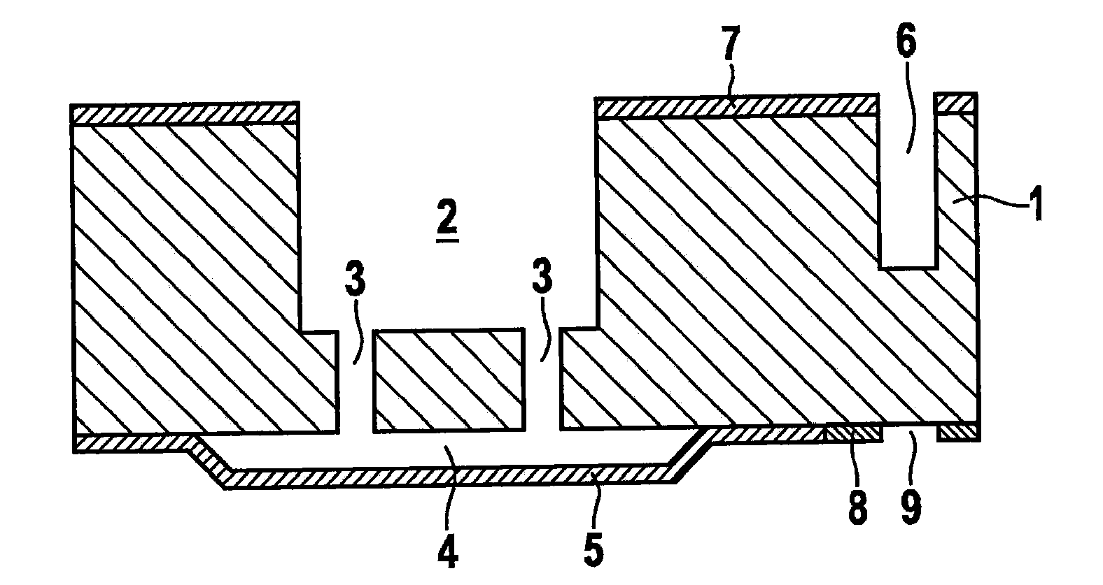
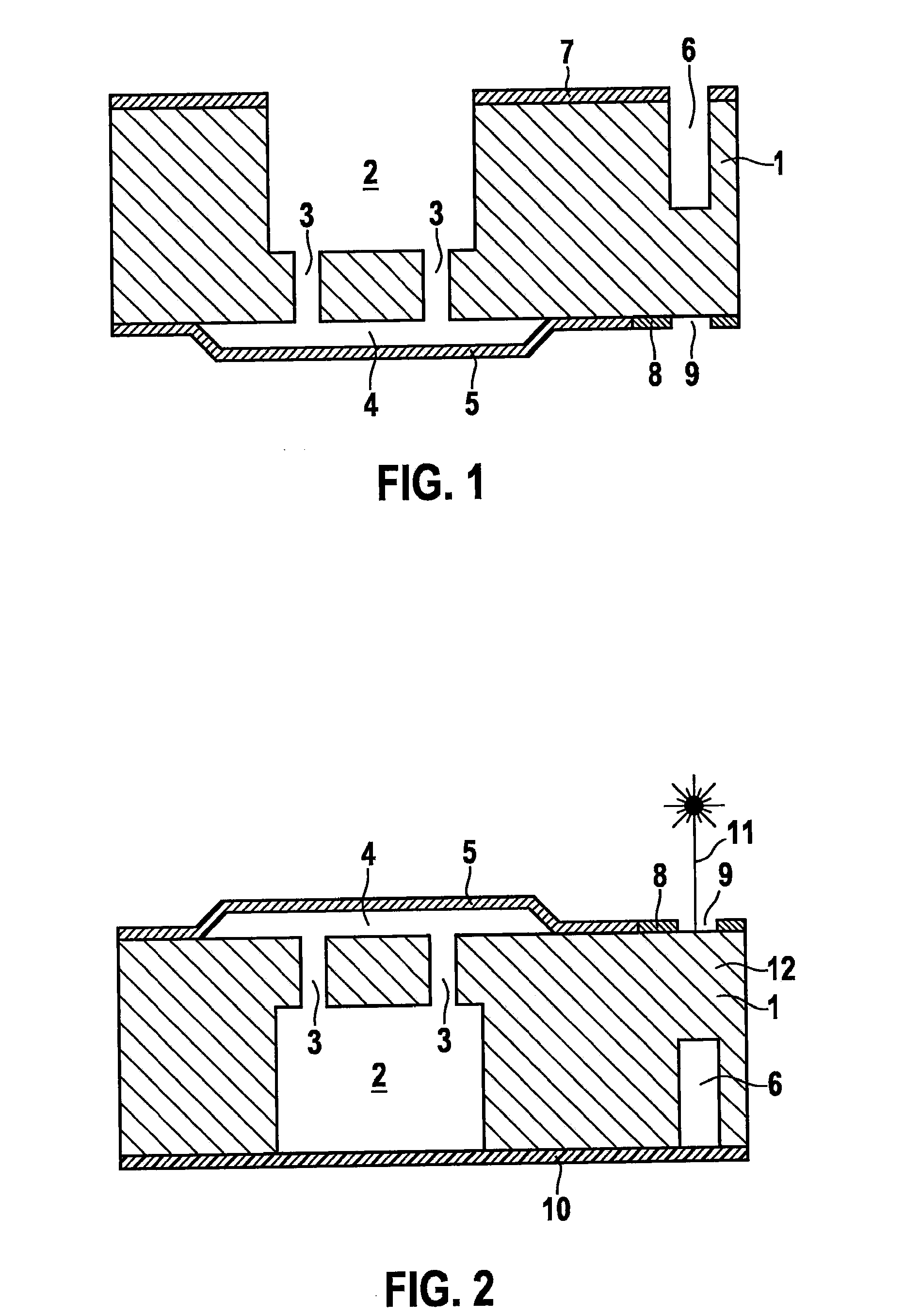
[0035]FIG. 1 shows a structured silicon wafer after the anisotropic plasma deep etching step. Silicon substrate 1 has been etched in such a way that cavity 2, perforation holes 3 through substrate 1, and hollow space 4 between substrate 1 and diaphragm 5 have been constructed. Furthermore, separation trenches 6 were applied at the same time as the etching of cavity 2. Cavity 2 and separation trenches 6 may fundamentally be produced having vertical side walls by the anisotropic etching process. Separation trench 6 is produced having a lesser etching depth than cavity 2 by utilizing the RIE lag effect. Residues of a masking layer 7 are still located on the side of substrate 1 facing away from the diaphragm. The surface of substrate 1 on the diaphragm side is partially covered by a further masking layer 8 at the points at which no diaphragm 4 is located. This masking layer 8 is interrupted by an unmasked area 9, however. Unmasked area 9 is in the extension of separation trench 6 and fi...


PUM


Abstract

A method for manufacturing separated micromechanical components situated on a silicon substrate includes the following steps of a) providing separation trenches on the substrate via an anisotropic plasma deep etching method, b) irradiating the area of the silicon substrate which forms the base of the separation trenches using laser light, the silicon substrate being converted from a crystalline state into an at least partially amorphous state by the irradiation in this area, and c) inducing mechanical stresses in the substrate. In one specific embodiment, cavities are etched simultaneously with the etching of the separation trenches. The etching depths can be controlled via the RIE lag effect.

Description

FIELD OF THE INVENTION[0001]The present invention relates to a method for manufacturing separated micromechanical components situated on a silicon substrate. Furthermore, the present invention relates to a micromechanical component which was manufactured by the foregoing method.BACKGROUND INFORMATION[0002]In the manufacture of micromechanical sensors having diaphragm structures of greatly varying functionality, the use of sawing to separate the chips of finished processed components represents a process known per se. For diaphragm manufacturing, in particular for microphones and pressure sensors, a cavity volume may be created on the rear side. In the case of closed diaphragms having a sealing function from the front side to the rear side and also a comparatively high mechanical stability, a conventional wafer sawing process may be applied without a particularly high risk of diaphragm damage. In the case of closed diaphragms, there is also not a high risk of irreversible sticking of...

Claims


Application Information

Patent Timeline
IPC IPC(8): H01L29/84H01L21/02
CPCB81C1/00888B81C2201/017G01L9/0042H04R31/006H01L21/30655H04R19/005H01L21/3065
Inventor LAERMER, FRANZTEEFFELEN, KATHRIN VANLEINENBACH, CHRISTINA
Owner ROBERT BOSCH GMBH
Why Eureka
Try Eureka