

Three Dimensional Integration and Methods of Through Silicon Via Creation
a three-dimensional integration and via technology, applied in the direction of semiconductor devices, semiconductor/solid-state device details, electrical devices, etc., can solve the problems of cost, process time, complexity, etc., and achieve the effect of improving the manufacturing process, reducing the cost of production, and improving the quality of production
- Summary
- Abstract
- Description
- Claims
- Application Information
AI Technical Summary
Benefits of technology
Problems solved by technology
Method used
Image

Examples
Embodiment Construction
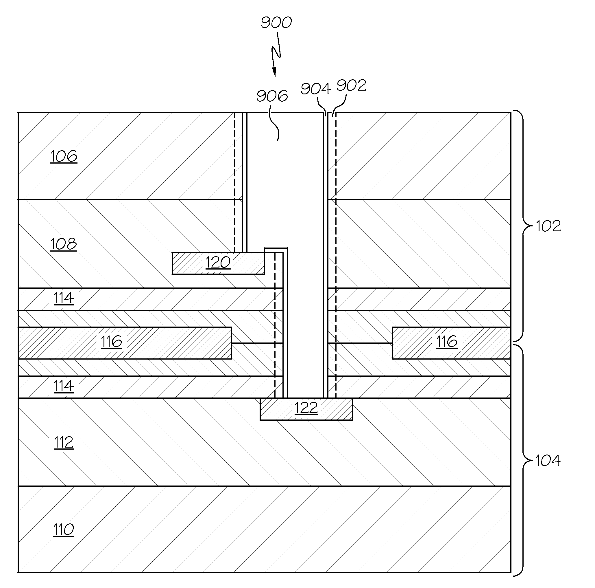
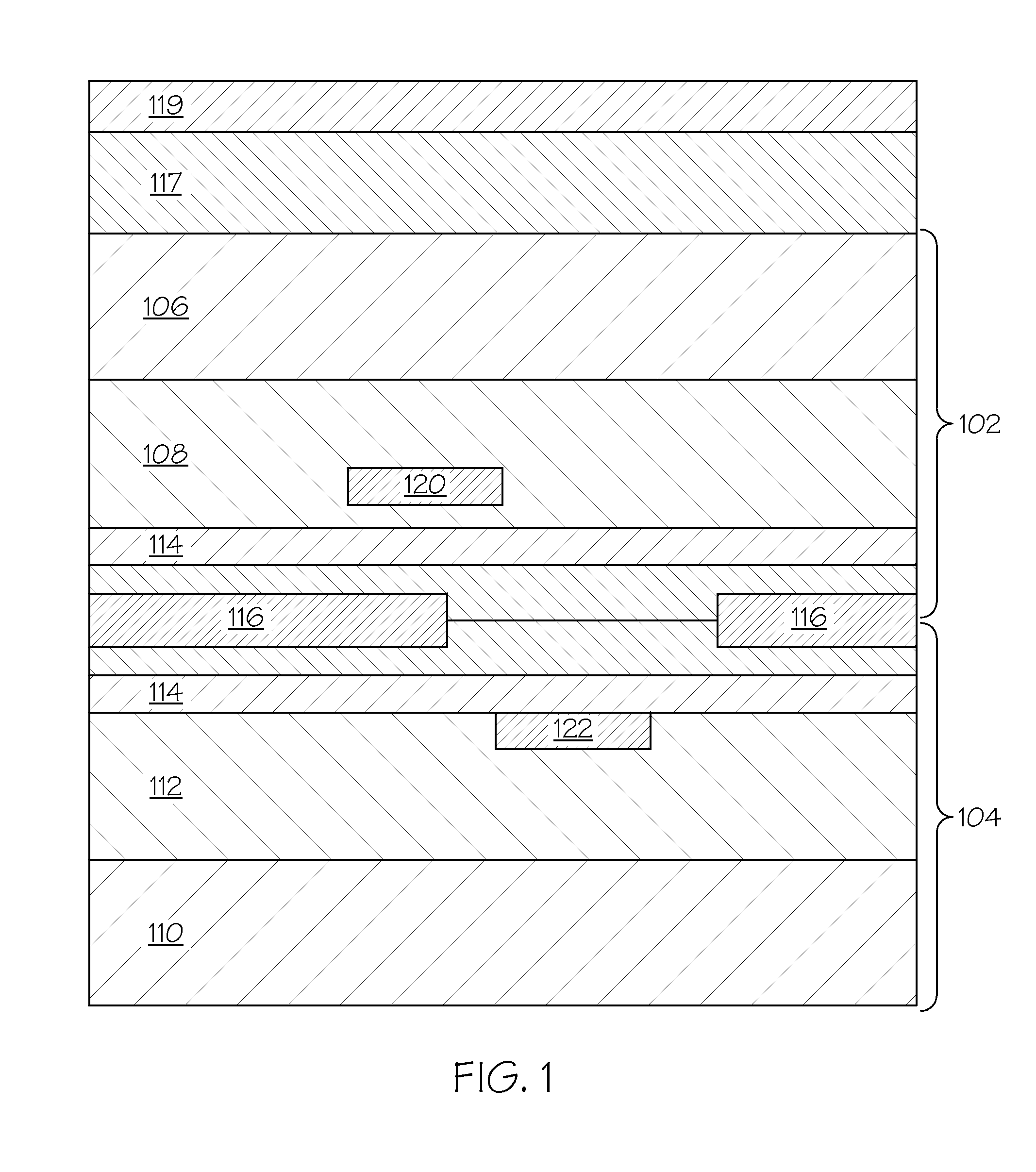
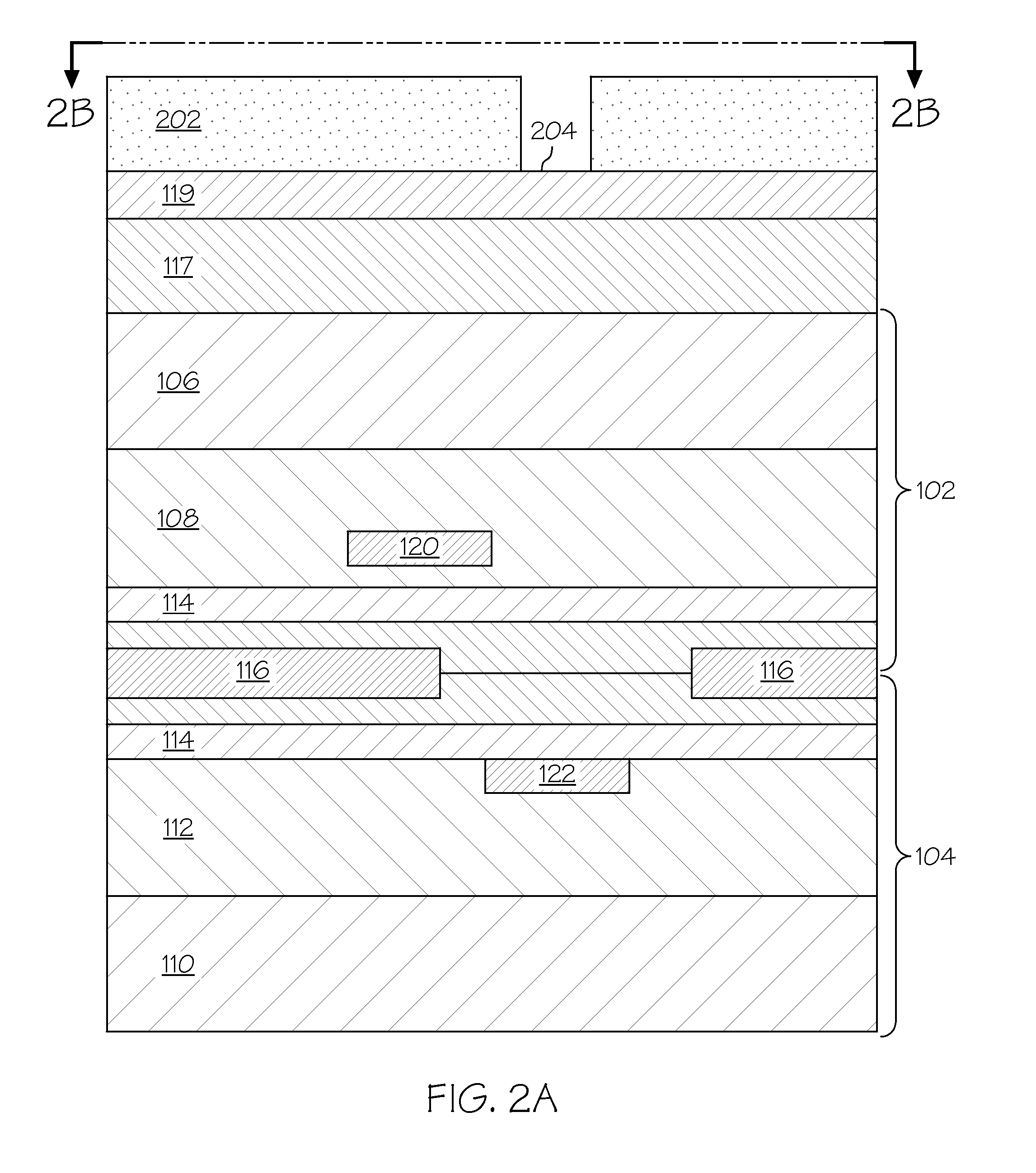
[0013]FIG. 1 illustrates a cross section view of an exemplary embodiment of a portion of a three-dimensional interconnect (3D IC) structure having a first component 102 arranged on a second component 104. The first component 102 and second component 104 may represent a portion of a silicon wafer or chip, in which the wafer or chip include a front-end-of-line (FEOL), middle-of-line (MOL), and back-end-of-line (BEOL) structures formed thereon, as known in the art. The first component 102 includes a substrate portion 106, and a wiring level portion 108, which may include, for example, a conductive line embedded in a dielectric layer. The substrate portion 106 includes a semiconductor material, which may be a single crystalline substrate which may be selected from, but is not limited to, silicon, germanium, silicon-germanium alloy, silicon carbon alloy, silicon-germanium-carbon alloy, gallium arsenide, indium arsenide, indium phosphide, III-V compound semiconductor materials, II-VI comp...
PUM
 Abstract
Description
Claims
Application Information