Organic electric field light-emitting element

a technology of organic electric field and light-emitting element, which is applied in the direction of organic semiconductor devices, thermoelectric devices, solid-state devices, etc., can solve the problems of large deviation in chromaticity of emitted light, insufficient improvement of permanence and emission efficiency of elements, and inability to achieve sufficient improvement of permanence and emission efficiency, reducing chromaticity deviation, and minimizing the effect of change in emission location

Active Publication Date: 2011-07-21
UDC IRELAND
View PDF3 Cites 22 Cited by
  • Summary
  • Abstract
  • Description
  • Claims
  • Application Information

AI Technical Summary

Benefits of technology

[0022]The present invention solves various problems in the art, and provides an organic electric field light-emitting element which has improved permanence and emission efficiency thereof, minimized change in the emission location, and reduced chromaticity deviation influenced by electric current applied to the element.

Problems solved by technology

However in this proposal, electrons passed through the light emitting layer are accumulated at an interface between the light emitting layer and the hole transporting layer, and part of the accumulated electrons leak to the hole transporting layer, which cause reduction in permanence, and emission efficiency of the resulting element.
However in this proposal, the location of emission significantly moves depending on the value of the applied electric current, which causes large deviation in chromaticity of the emitted light due to optical interference.
Especially in the case of a blue organic electric field light-emitting element, there is a problem that the permanence and emission efficiency of the element cannot be sufficiently improved as well as having the problem of the large deviation in the chromaticity.

Method used


Image

  • Organic electric field light-emitting element
  • Organic electric field light-emitting element
  • Organic electric field light-emitting element

Examples


example 1

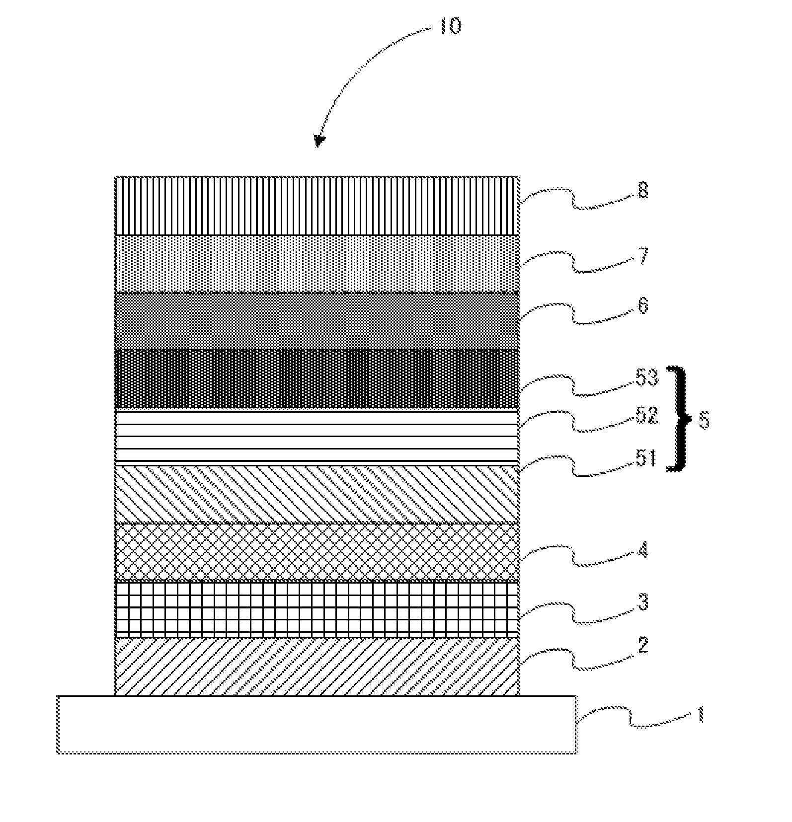
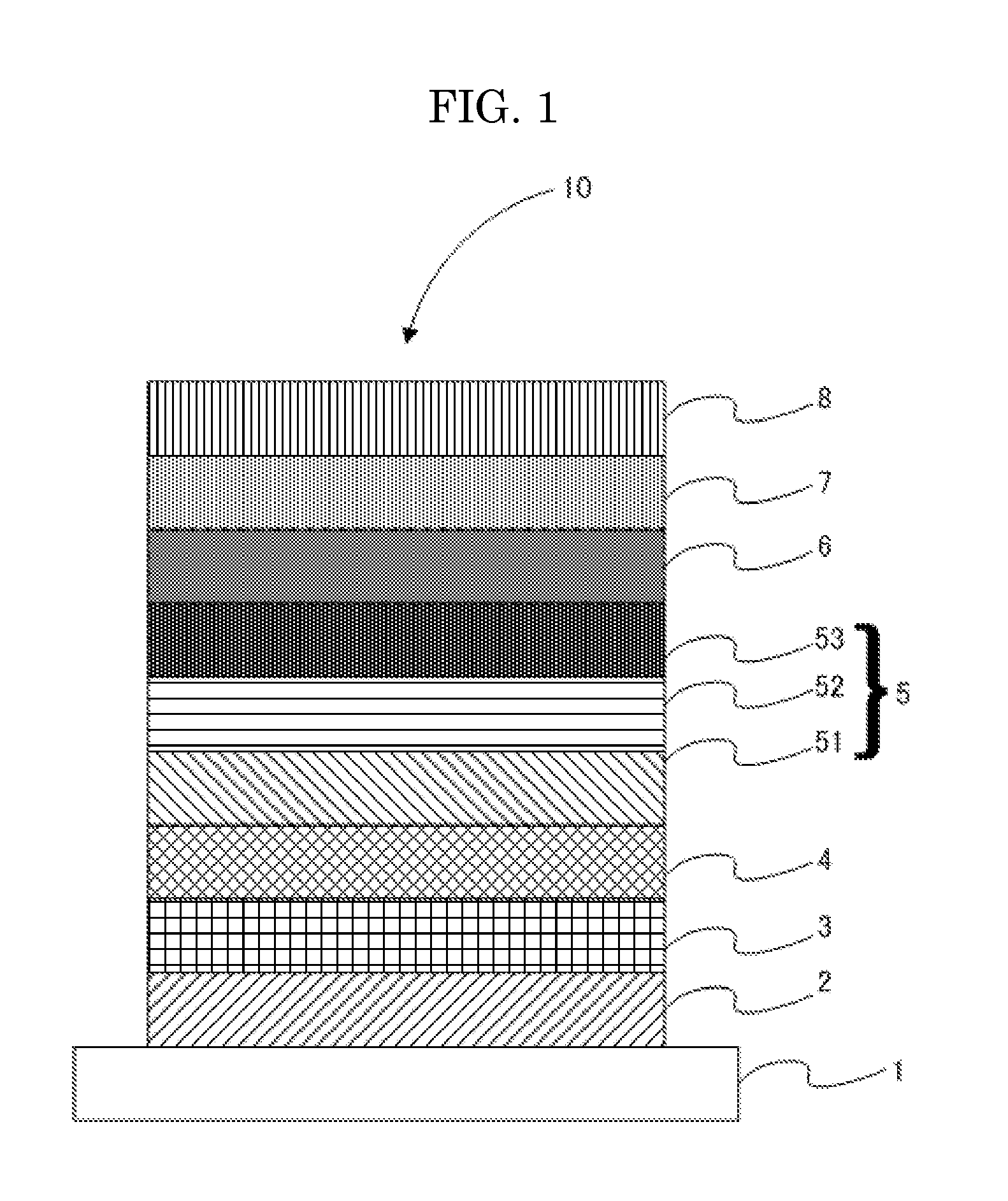
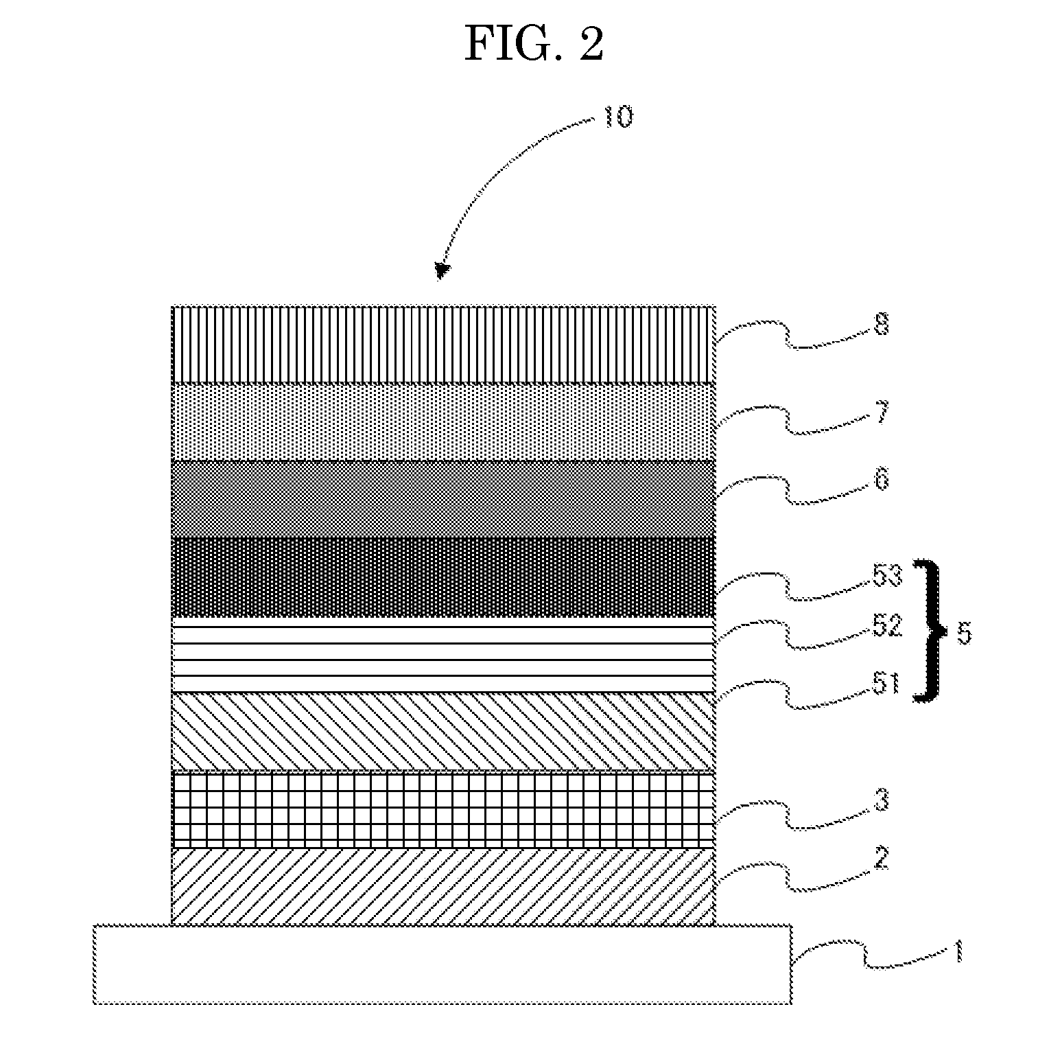
[0196]After placing a glass substrate having a thickness of 0.5 mm and a side of 2.5 cm in a wash container and washing in 2-propanol by ultrasonic cleaning, the glass substrate was subjected to UV-ozone treatment for 30 minutes. On this glass substrate, the following layers were deposited by vacuum deposition. Note that, in Examples and Comparative Examples below, the deposition rate was 0.2 nm / sec, unless otherwise stated. The deposition rate was measured by means of a crystal oscillator. Moreover, thicknesses of the following layers were measured by means of a crystal oscillator.

[0197]At first, as an anode, indium tin oxide (ITO) was provided on the glass substrate by sputtering to have a thickness of 70 nm.

[0198]Then, as a hole injection layer, the compound expressed by the following structural formula (Ir complex G-1) was deposited on the anode (ITO) to have a thickness of 10 nm.

[0199]On the hole injection layer, a first organic layer (serving as a hole transporting layer as we...

example 2

[0212]An organic electric field light-emitting element of Example 2 was prepared in the same manner as in Example 1, provided that the first organic layer was changed to contain 84% by mass of Compound 1, 15% by mass of Ir complex G-1, and 1% by mass of Pt complex G-1 as the electron-trapping material, relative to the mass of the first organic layer.

[0213]The prepared organic electric field light-emitting element was evaluated in terms of its driving voltage, external quantum efficiency, permanence, chromaticity change (Δ chromaticity), triplet level (T1) of the hole-blocking material, and triplet level (T1) of the hole-transporting phosphorescent material in the same manner as in Example 1.

example 3

[0214]An organic electric field light-emitting element of Example 3 was prepared in the same manner as in Example 2, provided that in the first organic layer the amount of Compound 1, the amount of Ir complex G-1 and the amount of Pt complex G-1 were respectively changed to 82% by mass, 15% by mass, and 3% by mass relative to the mass of the first organic layer, and in the second organic layer the amount of Compound 1, the amount of Ir complex G-1 and the amount of Pt complex G-1 were respectively changed to 82% by mass, 15% by mass, and 3% by mass relative to the mass of the second organic layer.

[0215]The prepared organic electric field light-emitting element was evaluated in terms of its driving voltage, external quantum efficiency, permanence, chromaticity change (Δ chromaticity), triplet level (T1) of the hole-blocking material, and triplet level (T1) of the hole-transporting phosphorescent, material in the same manner as in Example 1.


PUM


Abstract

An organic electric field light-emitting element, containing an anode; a cathode; and an organic layer provided therebetween and containing a first organic layer, a second organic layer and a third organic layer laminated in this order from the anode side, wherein the first organic layer contains a first host material in an amount of 10 to 90 mass % and a first hole-transporting phosphorescent material in an amount of 10 to 90 mass %; the second organic layer contains a second host material in an amount of 65 to 96.9 mass %, a second hole-transporting phosphorescent material in an amount of 3 to 30 mass %, and an electron-trapping material in an amount of 0.1 to 5 mass %; the third organic layer contain a hole-blocking material whose T1 is higher than that of the second hole-transporting phosphorescent material by at least 0.1 eV, wherein the second host material, the second hole-transporting phosphorescent material, and the electron-trapping material satisfy the following relationship:
|HOMOt2|>|HOMOh2|
|HOMOt2|>|HOMOp2|
|LUMOh2|+0.25 eV<|LUMOt2|
|LUMOp2|+0.25 eV<|LUMOt2|
and wherein the total average thickness of the first and second organic layers is at least 40 nm.

Description

BACKGROUND OF THE INVENTION[0001]1. Field of the Invention[0002]The present invention relates to an organic electric field light-emitting element (may also referred to as an “organic electroluminescence element”, an “organic EL element”, and the like).[0003]2. Description of the Related Art[0004]Organic electric field light-emitting elements have characteristics such as of self luminescence and high-speed response, and hence are expected as applications for flat panel displays. Especially since a two layer (laminate) type of organic electric field light-emitting elements, in which a thin hole-transporting organic film (i.e. a hole transporting layer) and a thin electron-transporting organic film (i.e. an electron transporting layer) are laminated were reported, organic electric field light-emitting elements attracted great deals of interests as large-scale luminescence elements which emits light with low voltage of 10 V or lower. The basic structure of the laminate type of the organ...

Claims


Application Information

Patent Timeline
Patent Type & Authority Applications(United States)
IPC IPC(8): H01L51/44
CPCH01L51/5004H01L2251/552H01L51/5016H10K50/11H10K2101/40H10K2101/10H10K2101/30
Inventor MASUI, KENSUKESOTOYAMA, WATARU
Owner UDC IRELAND
Why Eureka
Try Eureka