Interferometer, demodulator, and optical communication module

a technology of optical communication module and interferometer, which is applied in the direction of optical elements, instruments, transmission monitoring, etc., can solve the problems of shortening the optical phase modulation amount for a prescribed drive voltage, and shortening the system activation time, so as to achieve faster optical phase modulation speed, shorten the life of the device, and reduce the effect of strok

Active Publication Date: 2011-08-04
LUMENTUM JAPAN INC
View PDF18 Cites 13 Cited by
  • Summary
  • Abstract
  • Description
  • Claims
  • Application Information

AI Technical Summary

Benefits of technology

[0034]This makes it possible to minimize a stroke needed for the first optical phase modulation unit, i.e., a phase modulation range.
[0035]According to the present invention,

Problems solved by technology

Here, the inventor found a problem that, in conventional arts, system activation time becomes very long due to slow speed of the abovementioned optical phase modulation.
On the other hand, if the Piezo actuator in Patent Document 2 is used, it is possible to perform a optical phase modulation relatively faster and thereby shorten the system activation time, but property of the Piezo actuator is deteriorated by continuous activation thereof, causing a optical phase modulation amount for a prescribed drive voltage to decrease and eventually become insufficient.
This results in a problem that a lifetime of the delay line interferometer as an element, i.e., a time period during which the prescribed specifications are satisfied when it is used continuously, shortens.
In Patent Document 2, the delay line interferometer is made athermal and therefore f

Method used


Image

  • Interferometer, demodulator, and optical communication module
  • Interferometer, demodulator, and optical communication module
  • Interferometer, demodulator, and optical communication module

Examples


first embodiment

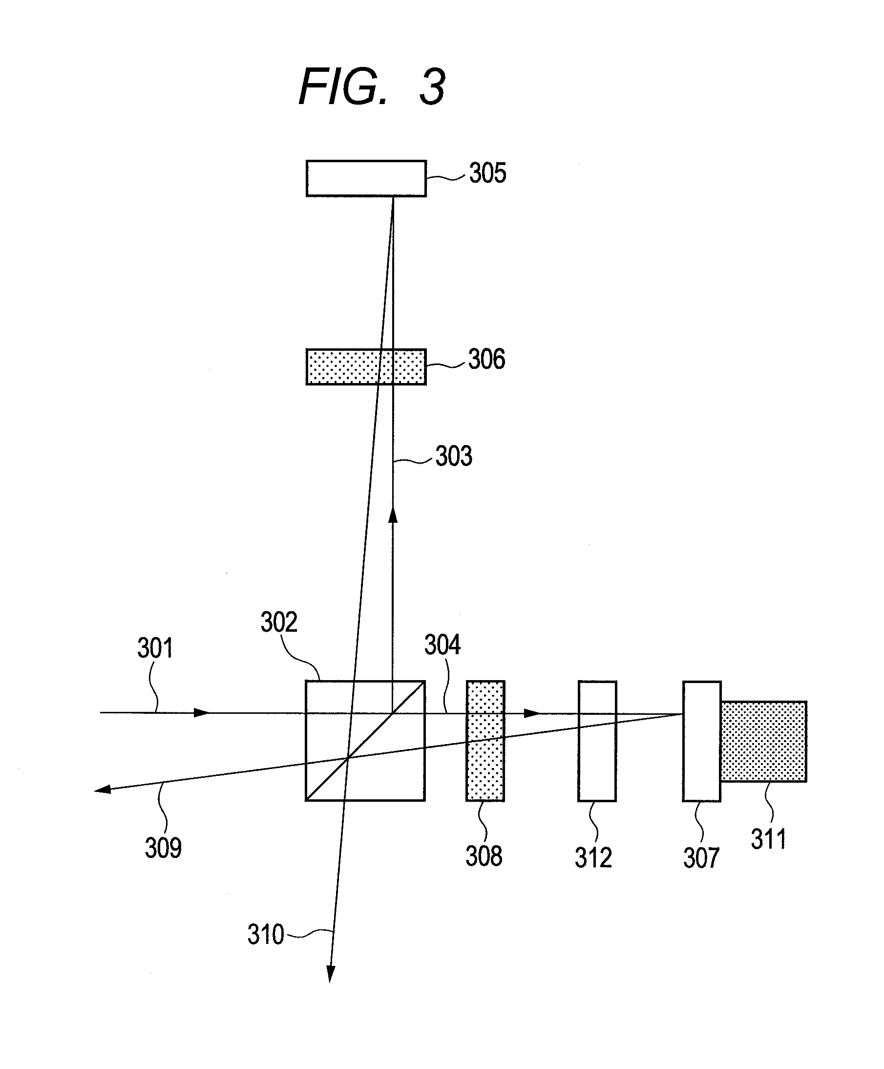
[0048]An embodiment of the present invention is described below with reference to FIG. 3.

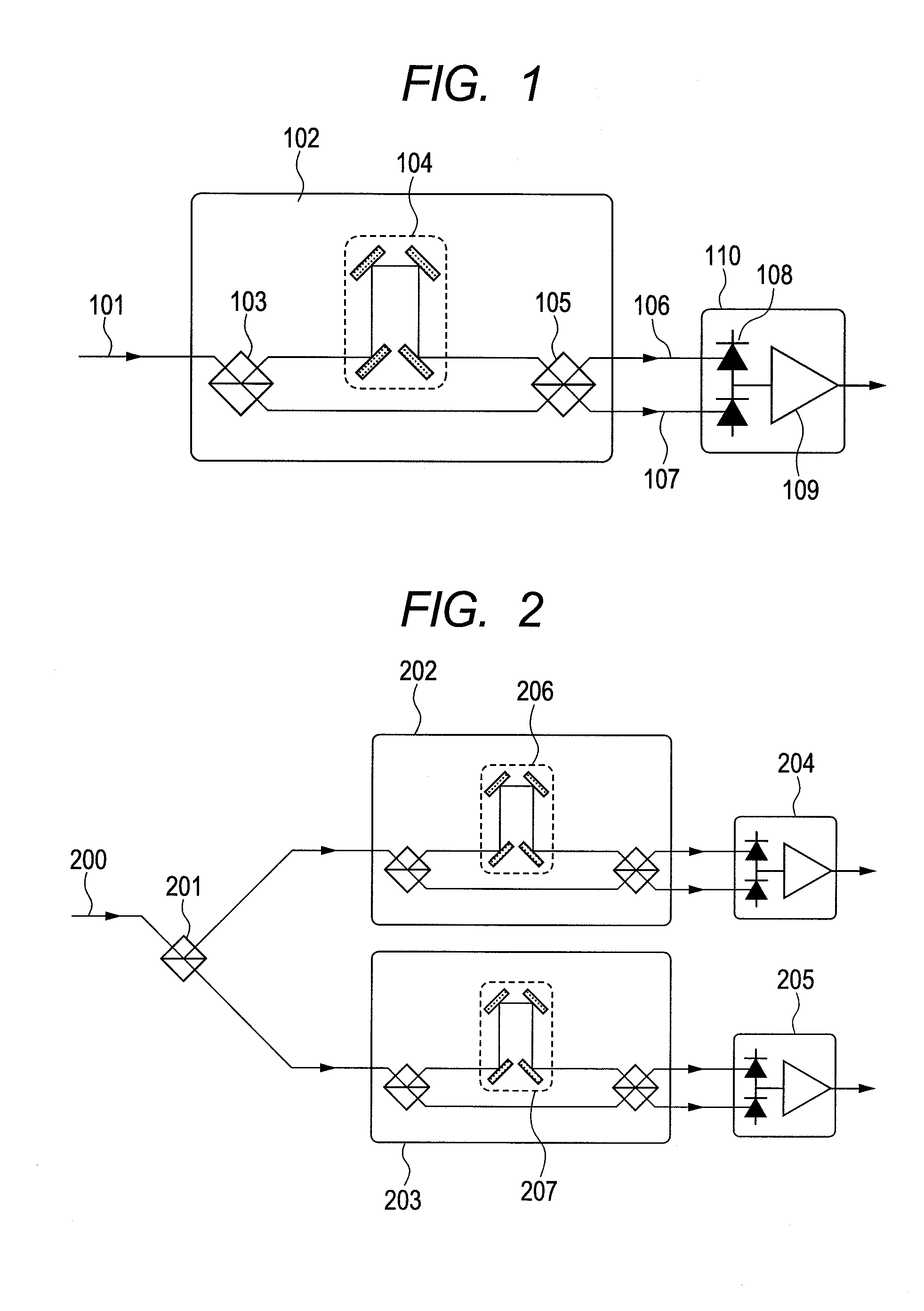
[0049]FIG. 3 shows a basic embodiment of the present invention. A modulated signal 301 that has been DPSK-modulated enters a half beam splitter 302 and is split into a first split light 303 and a second split light 304 at an intensity ratio of 1:1. The first split light 303 enters a mirror 305 at approximately 90 degrees and a reflected light from the mirror 305 enters the half beam splitter 302 again. Here, a quarter-wave plate 306 is inserted in outbound and inbound optical paths of the first split light and its fast axis is directed to a direction of 45 degrees relative to p-polarization that is defined by a separation plane of the half beam splitter 302. As a result, p-polarization component of the polarization of the first split light 303 is converted to s-polarization upon re-entering the half beam splitter 302, and likewise s-polarization component is converted to p-polarization component...

second embodiment

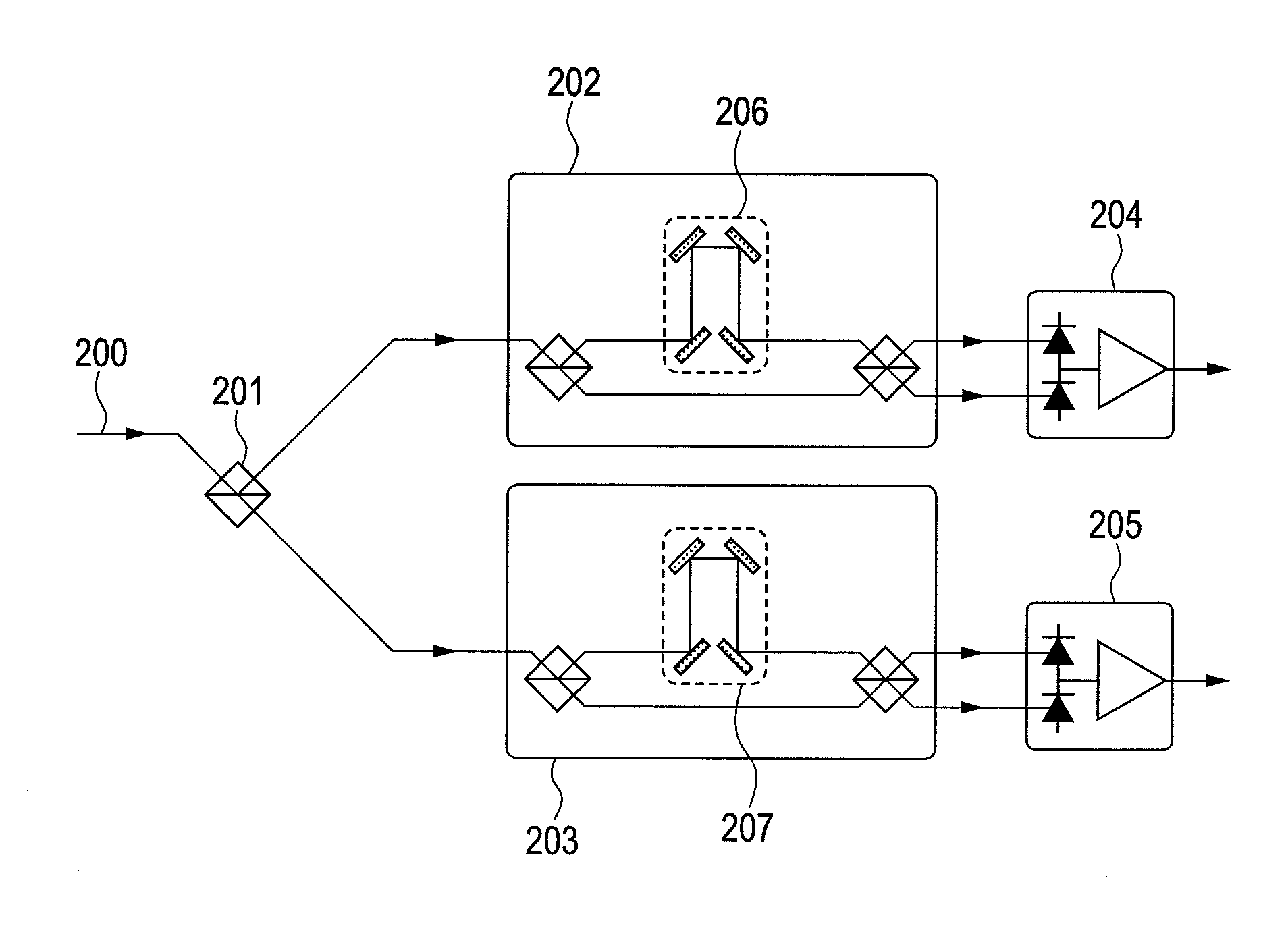
[0070]This embodiment is an embodiment in which the silicon monocrystal 312 in First Embodiment is replaced with a liquid crystal component. In this case, optical path length of the split light 304 changes due to a drive voltage for the liquid crystal component and thereby optical phase modulation is made possible. The liquid crystal component is one in which layers of equivalent thickness are glued together with their light axes crossed at 90 degrees, and it is possible to cause a phase difference not due to polarization of a split light. If a silicon monocrystal is used as in First Embodiment, large power consumption of several 100 mV to several watts is required for heating the silicon monocrystal with a heater or the like, but power consumption of a liquid crystal component is very small (1 mW or less) because an electric current hardly flows therein. Therefore, this embodiment allows for a small power consumption of the apparatus.

third embodiment

[0071]FIG. 7 is a view showing another embodiment in which optical phase modulation is done by thermal expansion of an expanding component on which a mirror reflecting one of split lights instead of the silicon monocrystal 312. In this case, an expanding component 701 is expanded by heating it and optical phase modulation is done by displacing a mirror 305. If wavelength of a light to be used as an example is 1550 nm, copper (linear expansion coefficient is used as an expanding component, and thickness of the expanding component is 5 mm, a change in optical path length when the expanding component is heated by 1° C. is 168 nm and a optical phase modulation of 0.68 radian is made. By performing a optical phase modulation with an expanding component that is not inserted in optical path as in this embodiment, it is possible to minimize the number of medium to be inserted in optical path, reduce the insertion loss of the apparatus, and facilitate the assembly adjustment.

[0072]Position o...


PUM


Abstract

When designing a demodulator for a DPSK-modulated signal, it is required that optical phase modulation is performed fast and the demodulator has a long lifetime. To achieve this object, a delay line interferometer inside the demodulator performs adjustment of phase difference between two split lights caused to interfere, using a first optical phase modulation unit such as a Piezo actuator and a second optical phase modulation unit such as a heating element that operates slower in modulation speed than the first optical phase modulation unit and is slower in deterioration speed.

Description

CLAIM OF PRIORITY[0001]The present application claims priority from Japanese patent application JP 2010-019875 filed on Feb. 1, 2010, the content of which is hereby incorporated by reference into this application.CROSS-REFERENCE TO RELATED APPLICATIONS[0002]This application is related to U.S. application Ser. No. 12 / 826,763 filed on Jun. 30, 2010, and U.S. application Ser. No. 12 / 896,948 filed on Oct. 4, 2010, the disclosure of which is hereby incorporated by reference.FIELD OF THE INVENTION[0003]The present invention relates to an interferometer, a demodulator that demodulates a differential phase-shift keying signal, and an optical communication apparatus (module) using it.BACKGROUND OF THE INVENTION[0004]In the optical communication field, a simplest scheme has been used that effects an intensity modulation as signal modulation and converts optical intensity directly into an electrical signal using a light detector. In recent years, however, a method of effecting phase modulation...

Claims


Application Information

Patent Timeline
IPC IPC(8): H04B10/08G02F1/01G02B26/06G01B9/02G02B26/00G02F1/061G02F2/00H04B10/516H04B10/548H04B10/61
CPCG02F1/061G02F1/01G02B26/00G02F2/00H04B10/677
Inventor MIKAMI, HIDEHARUKOGURE, TAICHI
Owner LUMENTUM JAPAN INC
Why Eureka
Try Eureka