

Semiconductor device and electronic appliance
a technology of semiconductor devices and electronic appliances, applied in the direction of optics, instruments, transportation and packaging, etc., can solve the problems of short channel effect, poor connection, and major defect generated in the manufacturing process, and achieve the effect of suppressing defects and favorable characteristics
- Summary
- Abstract
- Description
- Claims
- Application Information
AI Technical Summary
Benefits of technology
Problems solved by technology
Method used
Image

Examples
embodiment 1
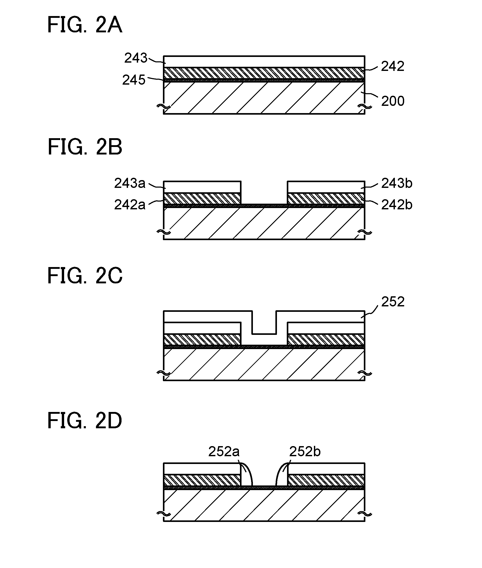
[0045]In this embodiment, an example of a structure of a semiconductor device and a manufacturing process according to one embodiment of the disclosed invention will be described with reference to FIG. 1, FIGS. 2A to 2D, and FIGS. 3A to 3E.
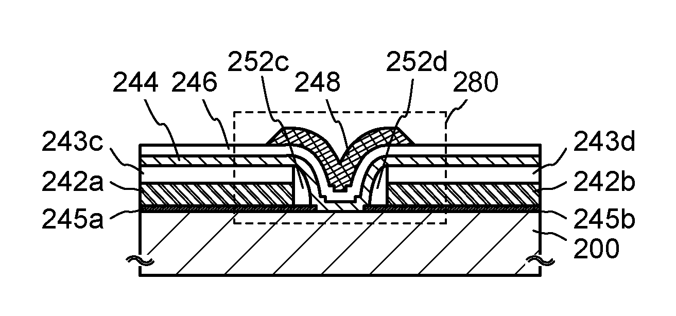
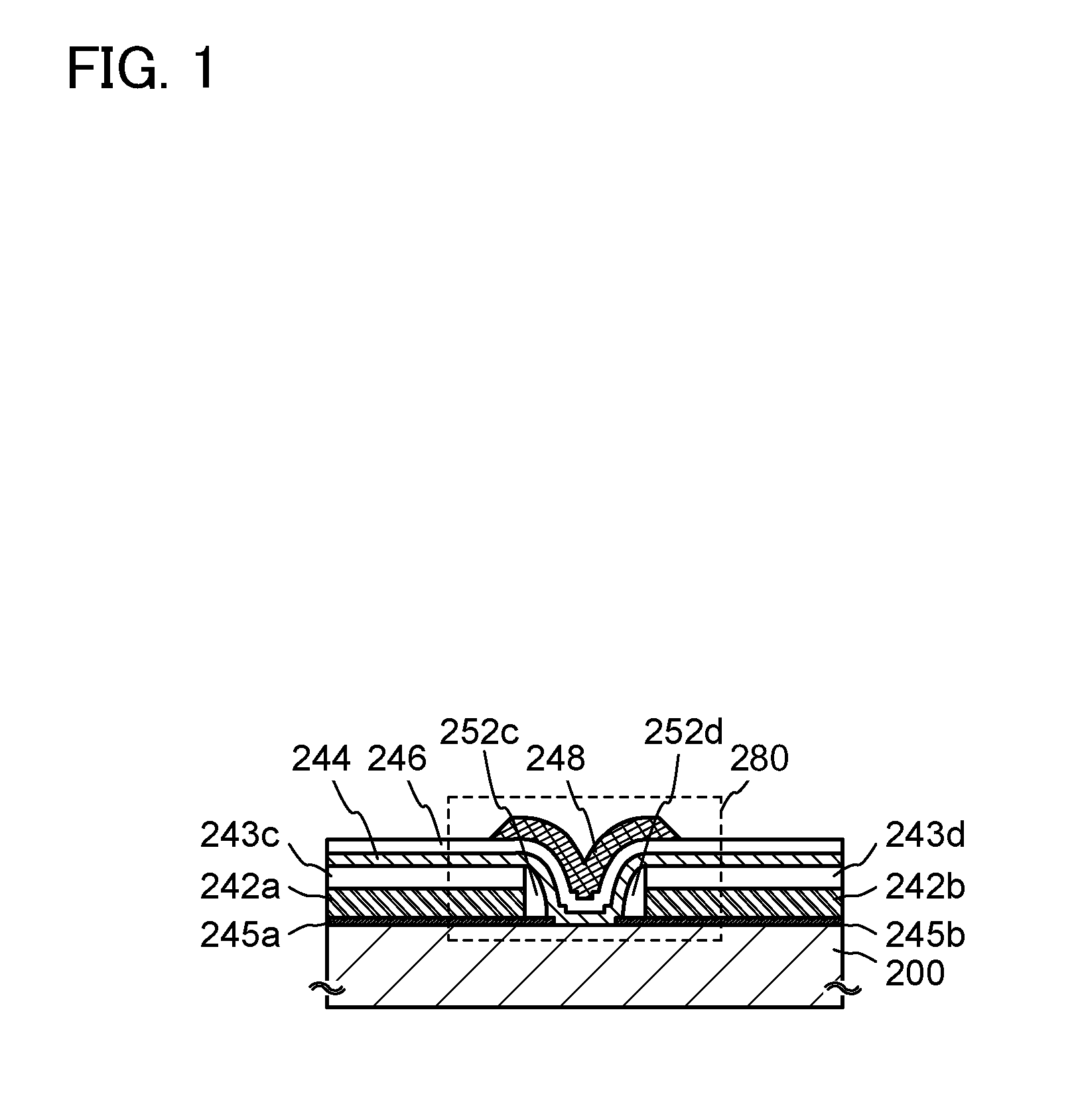
[0046]FIG. 1 illustrates a cross-sectional structure of a transistor as an example of a semiconductor device. In FIG. 1, a top-gate transistor is illustrated as a transistor according to one embodiment of the disclosed invention.
[0047]A transistor 280 illustrated in FIG. 1 includes, over a substrate 200, a source electrode in which a second conductive layer 245a and a first conductive layer 242a are sequentially stacked, a drain electrode in which a second conductive layer 245b and a first conductive layer 242b are sequentially stacked, a sidewall insulating layer 252c which is provided to be in contact with the source electrode, a sidewall insulating layer 252d which is provided to be in contact with the drain electrode, an insulating layer 243c ...
embodiment 2
[0109]In this embodiment, application examples of a semiconductor device according to another embodiment of the disclosed invention will be described with reference to FIGS. 4A-1, 4A-2, and 4B. Here, an example of a memory device is described. Note that in a circuit diagram, “OS” is written beside a transistor in order to indicate that the transistor includes an oxide semiconductor.
[0110]In the semiconductor device illustrated in FIG. 4A-1, a first wiring (a 1st line) is electrically connected to a source electrode of a transistor 300. A second wiring (a 2nd line) is electrically connected to a drain electrode of the transistor 300. A third wiring (a 3rd Line) is electrically connected to one of the source electrode and the drain electrode of the transistor 310, and a fourth wiring (a 4th Line) is electrically connected to a gate electrode of the transistor 310. A gate electrode of the transistor 300 and the other of the source electrode and the drain electrode of the transistor 310...
embodiment 3
[0149]In this embodiment, application examples of a semiconductor device according to another embodiment of the disclosed invention will be described with reference to FIGS. 5A and 5B, and FIGS. 6A to 6C.
[0150]FIGS. 5A and 5B are examples of circuit diagrams of semiconductor devices each including a plurality of semiconductor devices (hereinafter also referred to as memory cells 400) illustrated in FIG. 4A-1. FIG. 5A is a circuit diagram of a so-called NAND semiconductor device in which the memory cells 400 are connected in series, and FIG. 5B is a circuit diagram of a so-called NOR semiconductor device in which the memory cells 400 are connected in parallel.
[0151]The semiconductor device in FIG. 5A includes a source line SL, a bit line BL, a first signal line S1, a plurality of second signal lines S2, a plurality of word lines WL, and the plurality of memory cells 400. In FIG. 5A, one source line SL and one bit line BL are provided in the semiconductor device; however, one embodime...
PUM
 Abstract
Description
Claims
Application Information