

Sic semiconductor device and method of manufacturing the same
a semiconductor device and semiconductor technology, applied in semiconductor devices, semiconductor/solid-state device details, electrical equipment, etc., can solve the problem of significant accuracy control, and achieve the effect of suppressing the variation in the channel length
- Summary
- Abstract
- Description
- Claims
- Application Information
AI Technical Summary
Benefits of technology
Problems solved by technology
Method used
Image

Examples
embodiment 1
Preferred Embodiment 1
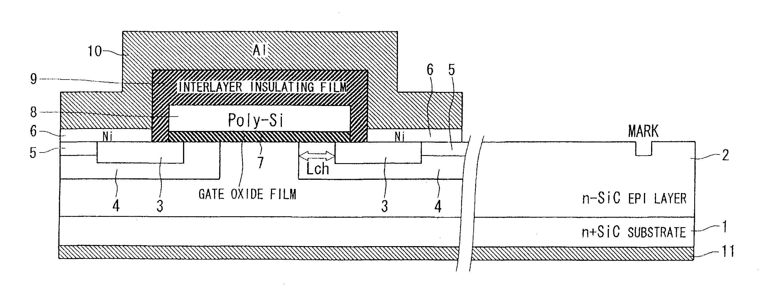
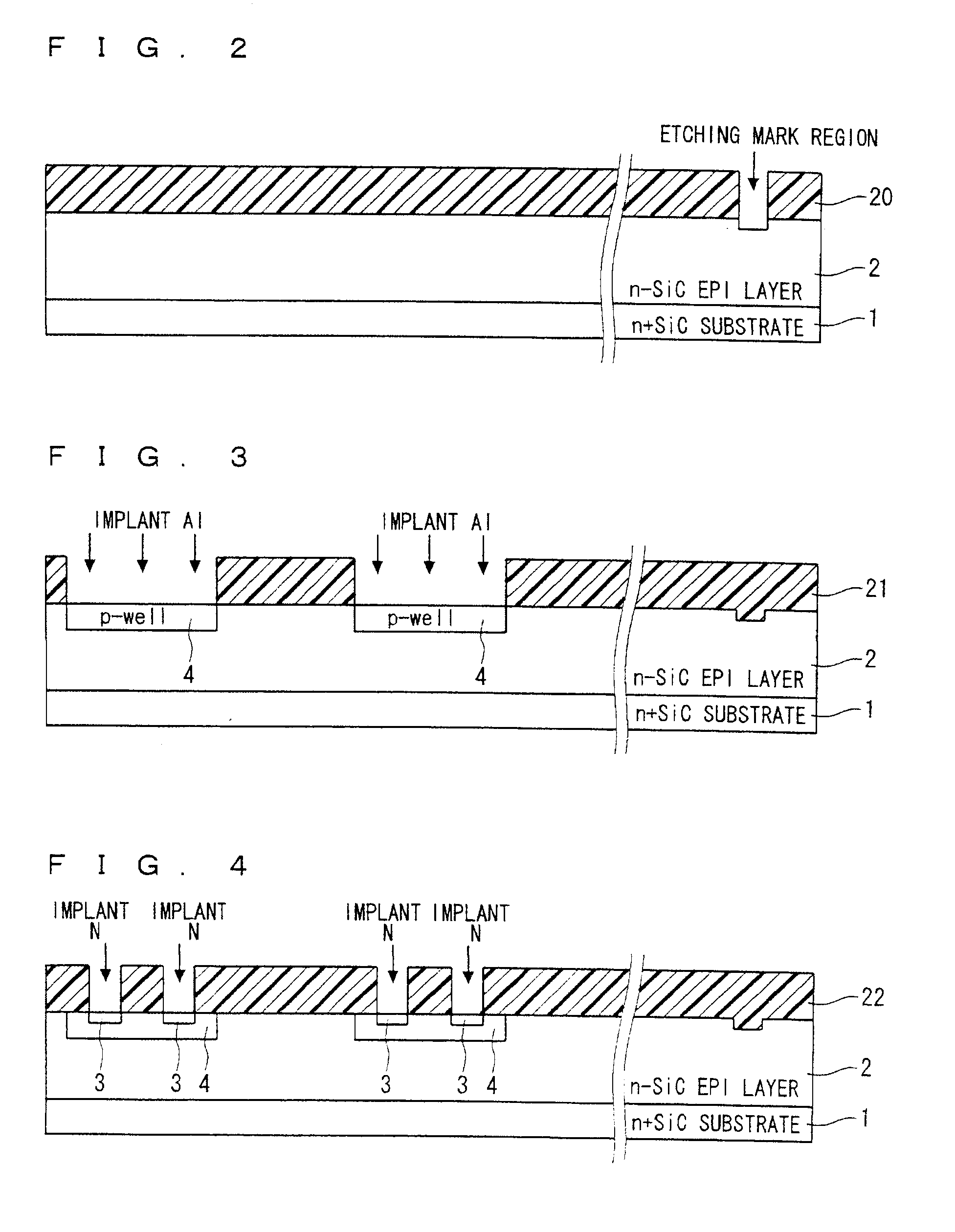
[0063]If the mark region and the source region 3 are simultaneously formed by performing etching and ion implantation by using a single mask, an etched portion of the source region 3 is formed without any misalignment from the reference mark region. If, in subsequent source forming steps, a mask alignment is performed by using the etched portion of the mark region or the source region 3, a variation in the channel length Lch can be suppressed because the source region 3 is formed without any misalignment from the mark region.
[0064]Along the procedure shown in FIGS. 7 to 11, a description will be given of an exemplary process of manufacturing a MOSFET in which etching and ion implantation for forming the mark region and the source region 3 are simultaneously performed. Firstly, by using a single mask 30, etching for the source region 3 and the mark region is performed on an SiC semiconductor layer including an n+SiC substrate 1 and an n−SiC epi layer 2 formed on...
PUM
 Abstract
Description
Claims
Application Information