Integrated sensor system

a sensor system and integrated technology, applied in the direction of converting sensor output, using electrical/magnetic means, instruments, etc., can solve the problems of introducing errors due to variation, and affecting the accuracy of measurement results

a sensor system and integrated technology, applied in the direction of converting sensor output, using electrical/magnetic means, instruments, etc., can solve the problems of introducing errors due to variation, and affecting the accuracy of measurement results

US20110193573A1Active Publication Date: 2011-08-11ASML NETHERLANDS BV

Image

  • Integrated sensor system
  • Integrated sensor system
  • Integrated sensor system

Examples


Embodiment Construction

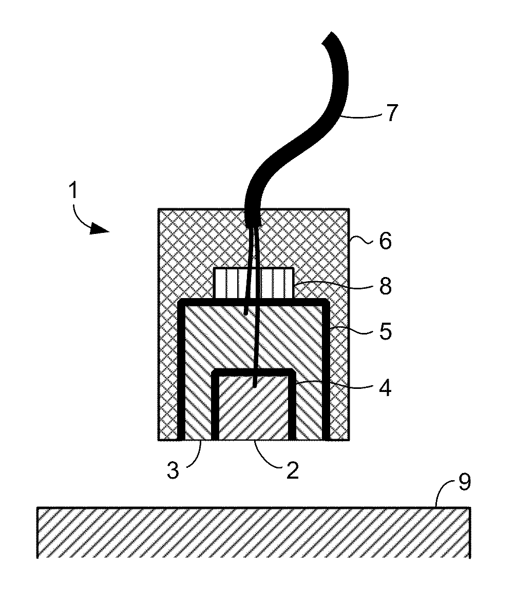
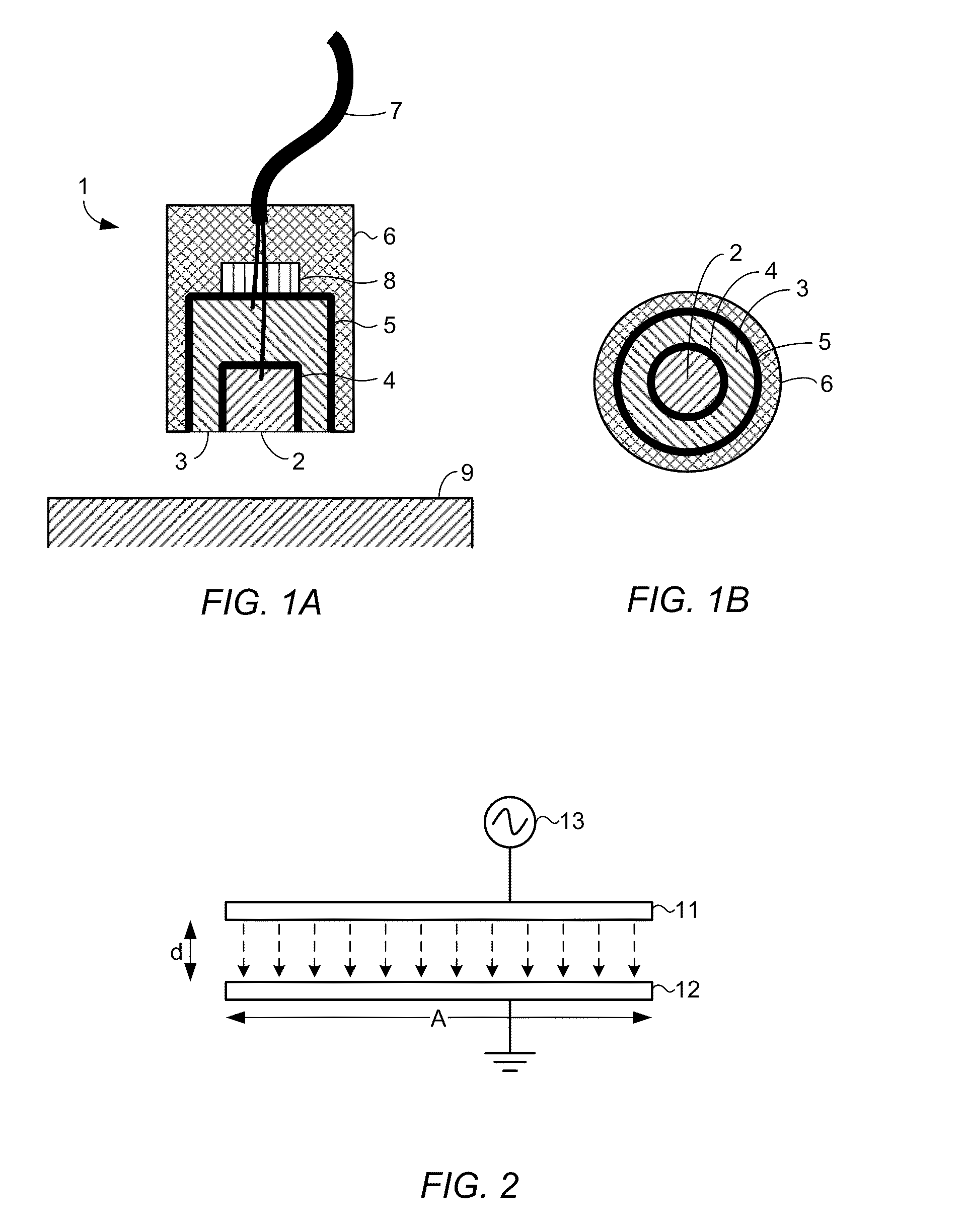
[0062]The following is a description of various embodiments of the invention, given by way of example only and with reference to the drawings.

Theory of Capacitive Sensors

[0063]A capacitive sensor uses a homogeneous electric field set up between two conductive surfaces. Over short distances, the applied voltage is proportional to the distance between the surfaces. Single-plate sensors measure the distance between a single sensor plate and an electrically conductive target surface.

[0064]FIG. 2 shows a parallel plate electrode arrangement. The capacitance between the two electrodes 11, 12 is given by the charge induced on one of the electrodes due to a potential difference between the two electrodes, divided by the potential difference, as represented in equation (1),

C=QΔV.(1)

[0065]The two parallel electrodes are separated by a distance d. Capacitance between the two electrodes is given by equation (2), neglecting the effects of field bending and non-homogeneity of the dielectric,

C=ɛ0ɛ...


PUM


Abstract

An integrated sensor system for a lithography machine, the system comprising a projection lens system (132) for focusing one or more exposure beams onto a target, a moveable table (134) for carrying the target (9), a capacitive sensing system (300) for making a measurement related to a distance between a final focusing element of the projection lens system (104) and a surface of the target (9), and a control unit (400) for controlling movement of the moveable table (134) to adjust a position of the target (9) based at least in part on a signal from the capacitive sensing system. The capacitive sensing system (300) comprises a plurality of capacitive sensors (30), each comprising a thin film structure. The capacitive sensors and the final focusing element (104) of the projection lens system are mounted directly to a common base (112), and the sensors are located in close proximity to an edge of the final focusing element of the projection lens system.

Description

BACKGROUND OF THE INVENTION[0001]1. Field of the Invention[0002]The present invention relates to a capacitive sensor for measuring distance, in particular capacitive sensor for measuring distance to a target in a lithography apparatus.[0003]2. Description of the Related Art[0004]Charged particle and optical lithography machines and inspection machines are used to expose patterns onto wafers and other targets, typically as part of a semiconductor device manufacturing process. In a lithography system a wafer is usually exposed at multiple locations by optical or particle exposure beams generated by the lithography machine. The wafer is usually positioned on a wafer table and multiple exposures are typically achieved by controlled displacement of the wafer table with respect to a stationary electron / optics column. The exposures are typically performed continuously on the wafer surface.[0005]The wafer surface which is to be exposed is almost never completely flat. A typical wafer may ha...

Claims


Application Information

Patent Timeline
11 Aug 2011
Publication
US20110193573A1
IPC
G01R27/26
CPC
G01B7/023; G01D3/036; G03F9/7053; G03F9/7026; G01D5/2417
Inventors
DE BOER, GUIDO; VAN BAAR, JOHNNY JOANNES JACOBUS