Power semiconductor device adaptive cooling assembly

a technology of adaptive cooling and semiconductor devices, which is applied in the direction of electrical apparatus casings/cabinets/drawers, domestic cooling apparatus, instruments, etc., can solve the problems of significant increase in the lifetime of the device, achieve the effect of enhancing the cooling efficiency of the heat sink, and reducing the switching frequency of the system

a technology of adaptive cooling and semiconductor devices, which is applied in the direction of electrical apparatus casings/cabinets/drawers, domestic cooling apparatus, instruments, etc., can solve the problems of significant increase in the lifetime of the device, achieve the effect of enhancing the cooling efficiency of the heat sink, and reducing the switching frequency of the system

US20110194256A1Active Publication Date: 2011-08-11KONINKLIJKE PHILIPS ELECTRONICS NV

Image

  • Power semiconductor device adaptive cooling assembly
  • Power semiconductor device adaptive cooling assembly
  • Power semiconductor device adaptive cooling assembly

Examples


Embodiment Construction

[0040]In the following, similar elements are denoted by the same reference numerals.

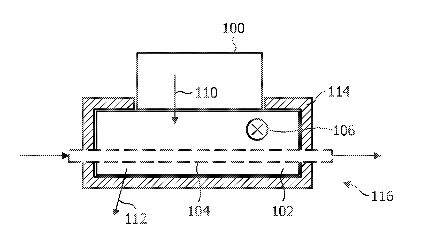
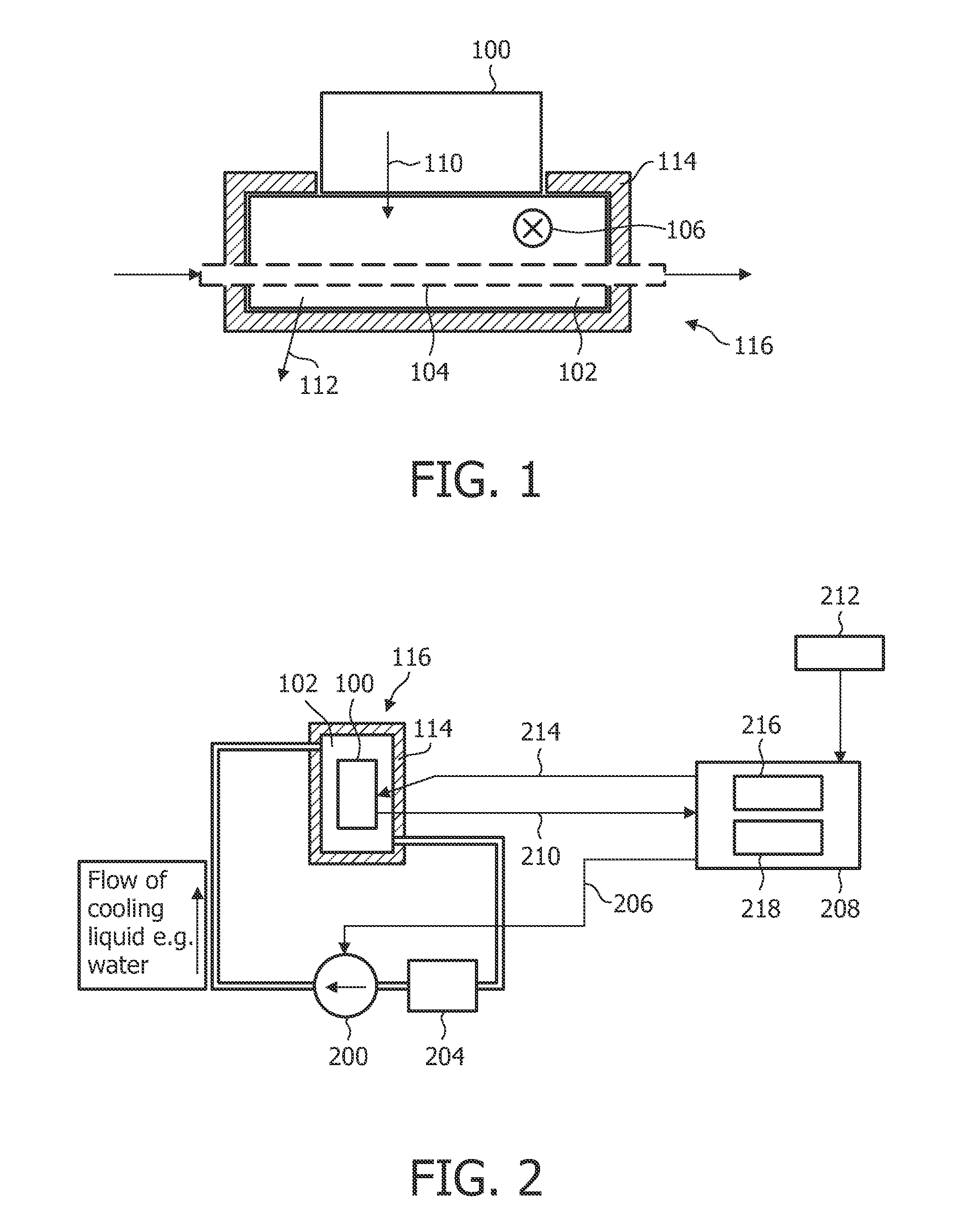
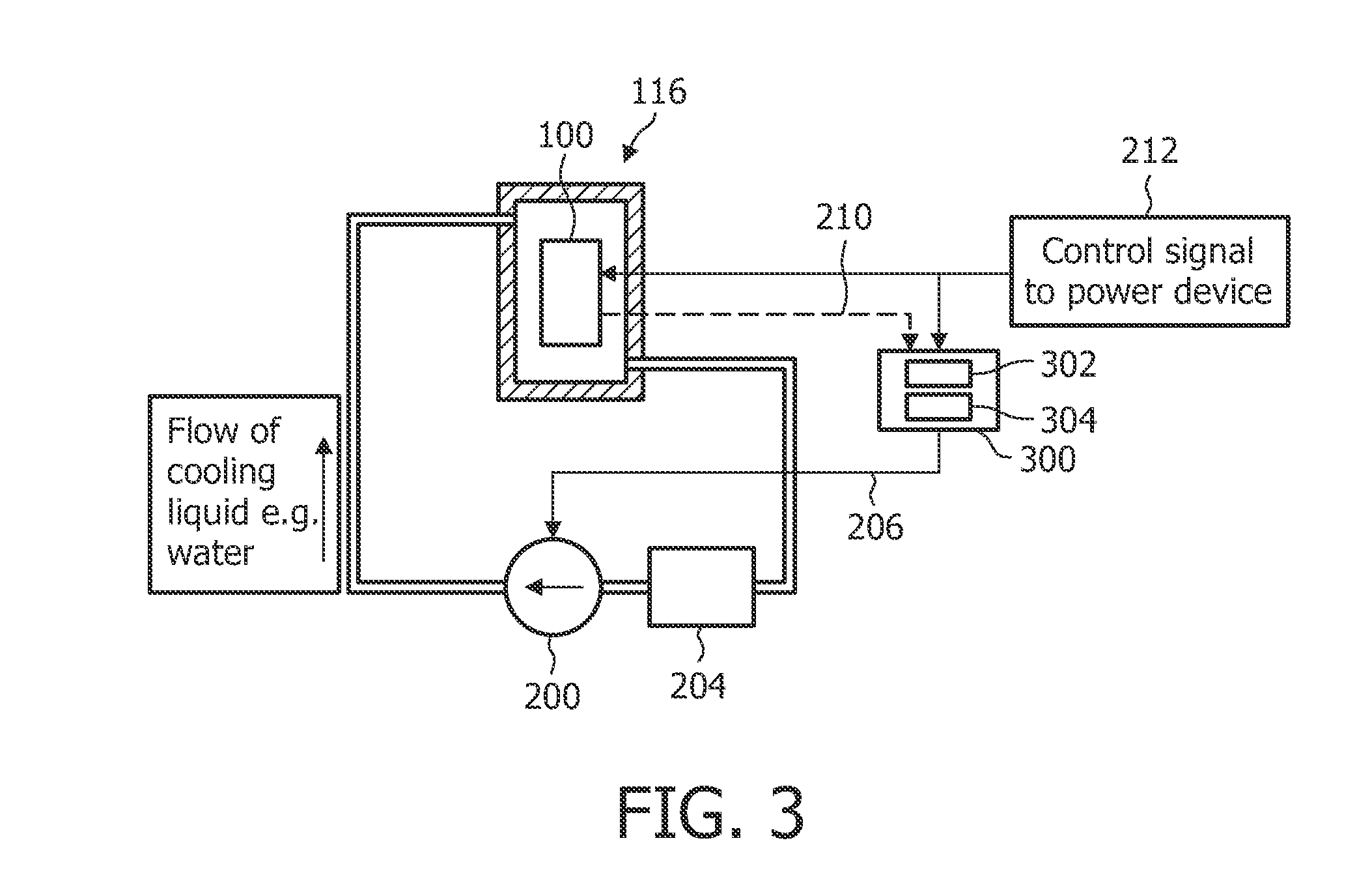
[0041]FIG. 1 shows a schematic illustrating an assembly 116 comprising a heat sink 102 on which a power semiconductor device 100, for example an IGBT is mounted. The heat sink 102 comprises a thermal insulation 114 which limits an unwanted heat flow to the environment to a minimum. As a consequence, a thermal equilibration is only performed between the power semiconductor device 100 by means of a heat flow 110 and by means of a thermal contact of the heat sink with an active cooling medium.

[0042]The active cooling may be for example performed by means of an airflow flowing in direction 106 through a plurality of fins (not shown here) of the heat sink 102, or by means of a tube 104 being in thermal contact with the heat sink 102 through which a cooling fluid is transported. As a consequence, the temperature of the power semiconductor device is determined by the thermal resistance between the semicondu...


PUM


Abstract

The invention relates to a power semiconductor device (100) cooling assembly for cooling a power semiconductor device (100), wherein the assembly comprises an actively cooled heat sink (102) and a controller (208; 300), wherein the controller (208; 300) is adapted for adjusting the cooling efficiency of the heat sink (102) depending on the temperature of the high current carrying semiconductor junction comprised in the power semiconductor device (100).

Description

TECHNICAL FIELD[0001]The invention relates to a power semiconductor device cooling assembly for cooling a power semiconductor device, a nuclear magnetic resonance examination system comprising a power semiconductor device cooling assembly, a method of operating a power semiconductor device cooling assembly and a computer program product.BACKGROUND AND RELATED ART[0002]Usually, power semiconductor devices are mounted onto large heat sinks with or without extra cooling measures, such as fan cooling or fluid cooling. Power semiconductor devices are semiconductor devices used as switches or rectifiers in power electronic circuits. Examples are power diodes, Thyristors, IGBTs (insulated gate bipolar transistors) and power MOSFETs.[0003]Heat sinks with or without extra cooling measures are designed in such a manner that in case of full power demand the temperature of the power semiconductor device remains below the absolute maximum as defined by its specifications. When the power demand i...

Claims


Application Information

Patent Timeline
11 Aug 2011
Publication
US20110194256A1
IPC
H05K7/20
CPC
H01L23/34; H01L2924/0002; H01L2924/00
Inventors
DE RIJCK, ALEXANDER CHRISTIAAN; HUISMAN, HENDRIK