Suspended Thin Film Structures

a thin film, suction technology, applied in the direction of layered products, transportation and packaging, chemistry apparatus and processes, etc., can solve the problems of large but dirty and often cracked graphene sheets, requiring either delicate or cumbersome processing, and requiring a large amount of processing. to achieve the effect of strengthening the bond

Inactive Publication Date: 2011-08-18
RGT UNIV OF CALIFORNIA
View PDF12 Cites 80 Cited by
  • Summary
  • Abstract
  • Description
  • Claims
  • Application Information

AI Technical Summary

Benefits of technology

[0028]Next, in a step (c), a solvent such as isopropanol (IPA) is applied to the structure so that it wets the amorphous carbon and the graphene layers; it is evaporated to bond these two layers. The sample is also baked (e.g. 10-20 min. on a hot plate at 120° C.) to strengthen the bond.

Problems solved by technology

These methods, however, require either delicate or cumbersome processing.
Such a small target window makes sample preparation difficult and unreliable.
However, these methods require several wet chemical steps that introduce contamination and mechanical damage, resulting in large but dirty and often cracked graphene sheets.
Further, such methods do not necessarily result in a strong bond between the graphene and the target substrate, and poor adhesion may result in unstable graphene TEM supports.

Method used


Image

  • Suspended Thin Film Structures
  • Suspended Thin Film Structures
  • Suspended Thin Film Structures

Examples


example 1

Preparation of a Graphene—Holey Carbon Grid Useful as a TEM Support

Preparation of a Graphene ATF on a Copper Foil Substrate

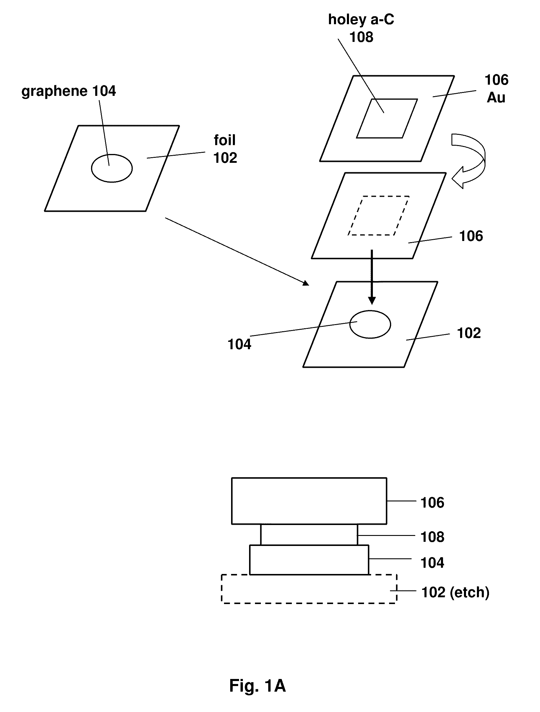
[0074]The direct transfer process begins with layer-area graphene growth on a Cu foil (Alfa Aesar #13382, 25 microns thick) via low-pressure chemical vapor deposition (See FIGS. 1 and 2).

Assembling the ATF-Substrate on a Carbon Grid Support so that the Graphene and Carbon are in Contact A hole-bearing carbon support over a target TEM grid (SPI Au Quantifoil with 1.2 um holey amorphous-C, (“a-C) film) is placed on top of the graphene on Cu, such that the a-C film faces down towards the graphene. Other forms of mesh on foil TEM supports may be obtained or used. These are sold e.g., by Ted Pella, Inc. Redding, Calif. See, FIG. 1A.

Adhering the ATF Graphene to the Carbon Grid

[0075]A drop of isopropanol (IPA) is gently placed on top of the grid, wetting both the grid's a-C film and the underlying graphene film. As the IPA evaporates, surface tension draws the graphene...

example 2

Characterization of Graphene TEM Grids

[0078]Characterization of direct transfer graphene TEM grids is performed on a JEOL 2010 TEM operated at 100 kV. FIG. 3 shows the graphene grid prepared in Example 1 at different magnifications. Macroscopic grid-wide graphene coverage is apparent in FIG. 3A, an optical micrograph captured near the end of the evaporative adhesion step. Darker regions in this image show where graphene has bonded to the a-C support. FIG. 3B, a subset of a grid frame captured by TEM, reveals large unperturbed graphene sheets with occasional folds and cracks. FIG. 3C shows a higher magnification image of a single graphene domain covering an a-C hole. FIG. 4A shows a typical view of the suspended graphene, with large (tens of nanometers) atomically clean regions separated by scattered amorphous and / or organic materials covering the highly reactive graphene surface, rivaling the cleanliness seen earlier with exfoliated graphene flakes transferred to TEM grids and descr...

example 3

Photolithographic Patterning to Selectively Etch Cu Growth Substrates: an Alternate Route to Suspended Graphene Architectures

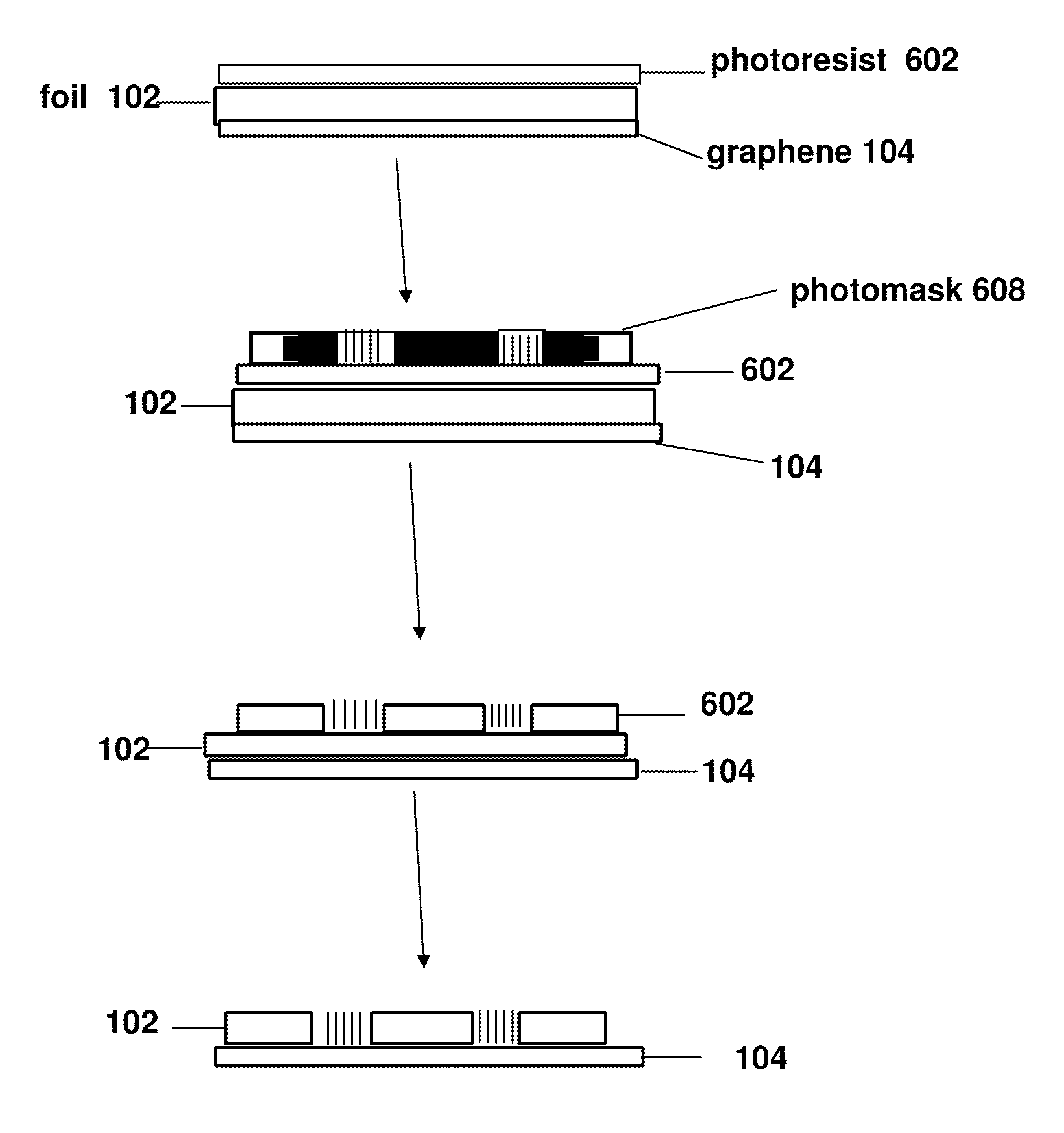
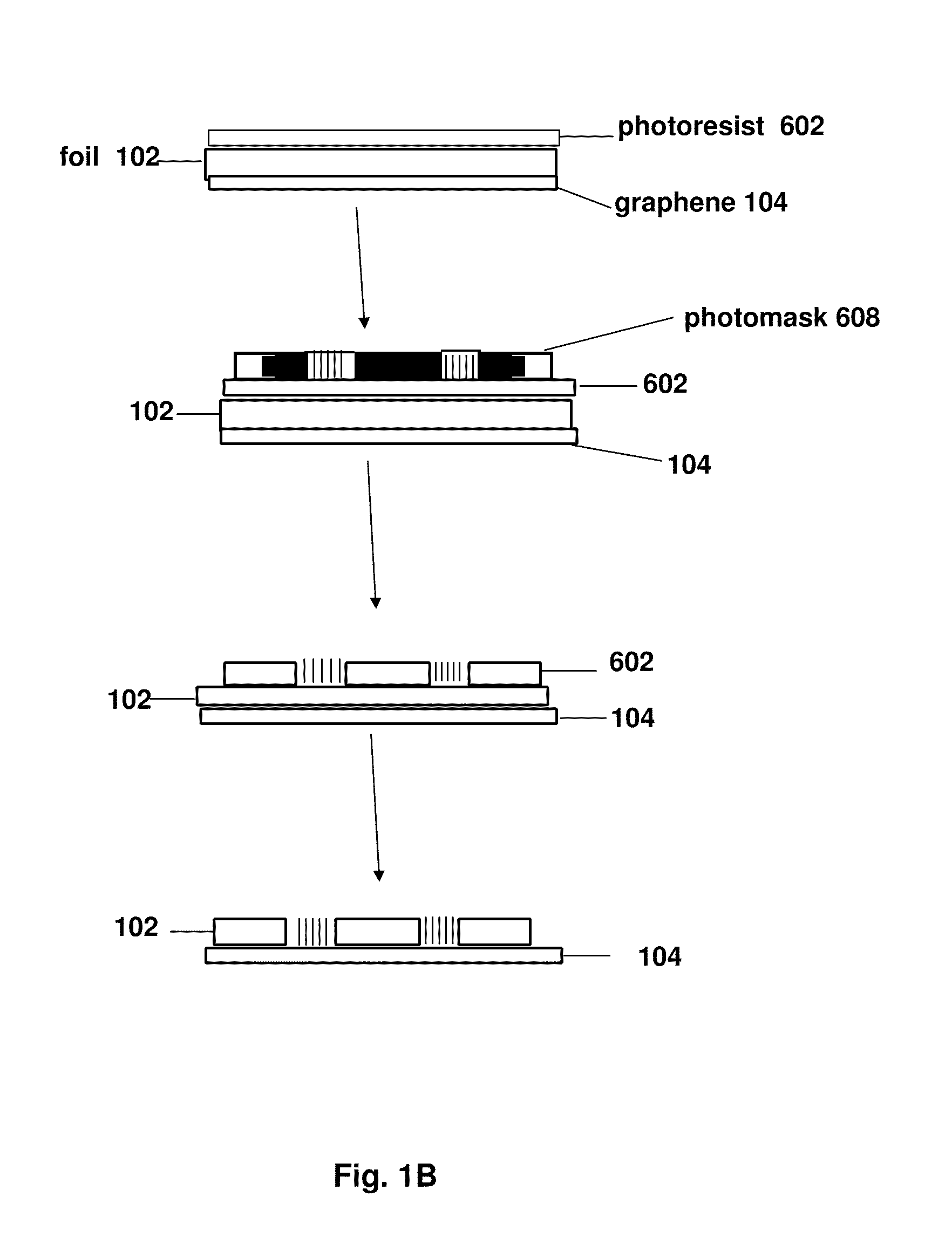
[0082]As shown in FIG. 6A, foil 102 is layered with graphene 104 as previously described. A layer of photoresist 602 (FIG. 6B) is applied to the copper foil layer. FIG. 6C shows a photomask containing the structure of the entire TEM grid (scaffolding, outer support ring, etc.) being placed over the substrate. As is known in the art of photolithography, UV light is shined on the structure through the mask 608. (The photomasks can be designed to have arbitrary geometric layout; for instance, a mask containing an indexed pattern array—a reference grid—can be made to facilitate the characterization of the same region of the grid for experiments involving a series of processing or modifications to a sample). The exposed photoresist is then removed (FIG. 6D) when the substrate is soaked in photoresist developer; after copper etching, the remaining photoresist is rem...


PUM

PropertyMeasurementUnit
sieve opening sizeaaaaaaaaaa
sizesaaaaaaaaaa

Abstract

Disclosed is a method of preparing a support structure suitable for use, e.g., in microscopic studies, comprising a free standing atomically thin film (e.g. graphene) suspended across an opening in the support structure. The method in one aspect comprises the steps of preparing a thin film which is an atomically thin film (e.g., graphene) on a surface of a solid substrate to form a graphene-layered substrate; attaching the graphene layer to a hole-containing support mesh; removing the solid support, thereby transferring the graphene layer from the substrate to the carbonaceous hole-containing layer on the support mesh; and then removing contaminants to obtain said structure. In another aspect, the present method does not involve a transfer, but comprises a lithography and etching process in which the atomically thin layer is applied to a support which is marked with a lithographic pattern and selectively etched, leaving the free standing film.

Description

CROSS-REFERENCE TO RELATED APPLICATIONS[0001]This application claims priority from U.S. Provisional Patent Application No. 61 / 298,326, filed on Jan. 26, 2010, which is hereby incorporated by reference in its entirety.[0002]REFERENCE TO SEQUENCE LISTING, COMPUTER PROGRAM, OR COMPACT DISK[0003]None.STATEMENT OF GOVERNMENTAL SUPPORT[0004]This invention was made with U.S. Government support under U.S. Department of Energy Contract Number DE-AC02-05CH11231. The Government has certain rights in this invention.BACKGROUND OF THE INVENTION[0005]1. Field of the Invention[0006]The present invention relates to the field of devices that comprise an atomically thin film or sheet (e.g., graphene) suspended across a hole or mesh openings, including such devices as made and adapted for use in supporting samples for transmission electron microscopy.[0007]2. Related Art[0008]Presented below is background information on certain aspects of the present invention as they may relate to technical features r...

Claims


Application Information

Patent Timeline
Patent Type & Authority Applications(United States)
IPC IPC(8): B32B9/00B32B37/02B32B37/14B32B38/10C23F1/00B32B3/10B82Y30/00
CPCB82Y30/00Y10T428/24331H01J37/20
Inventor REGAN, WILLIAM R.ZETTL, ALEXANDERALEMAN, BENJAMIN J.
Owner RGT UNIV OF CALIFORNIA
Why Eureka
Try Eureka