Mixer circuits for second order intercept point calibration

a mixing circuit and intercept point technology, applied in the field of radio frequency receivers, can solve problems such as the leakage of transmitter signals into the receiver's receive path, the inability to accurately calibrate the signal, and the inability to accurately detect the signal

Inactive Publication Date: 2011-08-18
NORTH STAR INNOVATIONS
View PDF30 Cites 11 Cited by
  • Summary
  • Abstract
  • Description
  • Claims
  • Application Information

AI Technical Summary

Problems solved by technology

If the LNA and the SAW filter are removed from the analog line-up of the receiver, problems that can detrimentally affect the performance of the receiver may arise.
In a transceiver, which comprises a transmitter and a receiver, one such problem is a signal transmitted by the transmitter leaking into a receive path of the receiver.
Without a sufficiently high IP2 of the mixer, the presence of second order intermodulation distortion (IMD2) substantially reduces the sensitivity of the receiver.
Non-idealities that affect IIP2 performance include device mismatch and layout asymmetry.
However known calibration techniques do not address temperature variation, can create significant DC offsets in the receiver path, can result in long calibration times that complicate system design, can degrade the noise figure, can degrade common-mode rejection ratio (CMRR) of a baseband operational amplifier (a reduction in the CMRR can significantly limit IIP2 calibration range), can be difficult or non-optimal to implement from a layout perspective, and can result in limited / inadequate calibration range.
Such an approach does not address the problem of IIP2 compensation over temperature.
The Gilbert cell mixer topology limits optimum achievable IIP2 performance as compared to a passive CMOS mixer and the manufacturing process cost is higher.
The second approach does not work with a double-balanced mixer topology.
The second approach is not applicable to rail-to-rail CMOS oscillator implementations, does not provide a rail to rail input to the mixer for optimum linearity, and does not provide common mode.
Some known mixers do not allow for a common-centroid layout while still maintaining each device of the mixer on a same bulk.
Lack of a common-centroid layout results in degraded matching and increased IIP2.
When a common-centroid layout can only be accomplished by disposing each device on a separate bulk, matching degrades because the separation between devices is greater.
A high DC offset is disadvantageously created if the common mode voltage offset is induced at the mixer input, such as at the source of mixer devices.
A resistor at the input adds noise to the lineup because an additional connection is unnecessarily made to the signal path.
If the common mode voltage offset is forced, through a resistor, at the mixer output, a high DC offset is disadvantageously created.
The resistor at the output adds noise to the lineup.
Each time a calibration is done a DC offset correction may be needed, which increases calibration time.
However, the DC offset becomes large at extreme settings of the post-mixer IIP2 calibration, which requires a large number of bits for IIP2 calibration D / A converter, and the technique disadvantageously requires that a DC offset correction algorithm be run after each IIP2 calibration.
Some mixers have a voltage-mode stage following the mixer, which is non-optimal for linearity.

Method used


Image

  • Mixer circuits for second order intercept point calibration
  • Mixer circuits for second order intercept point calibration
  • Mixer circuits for second order intercept point calibration

Examples


first embodiment

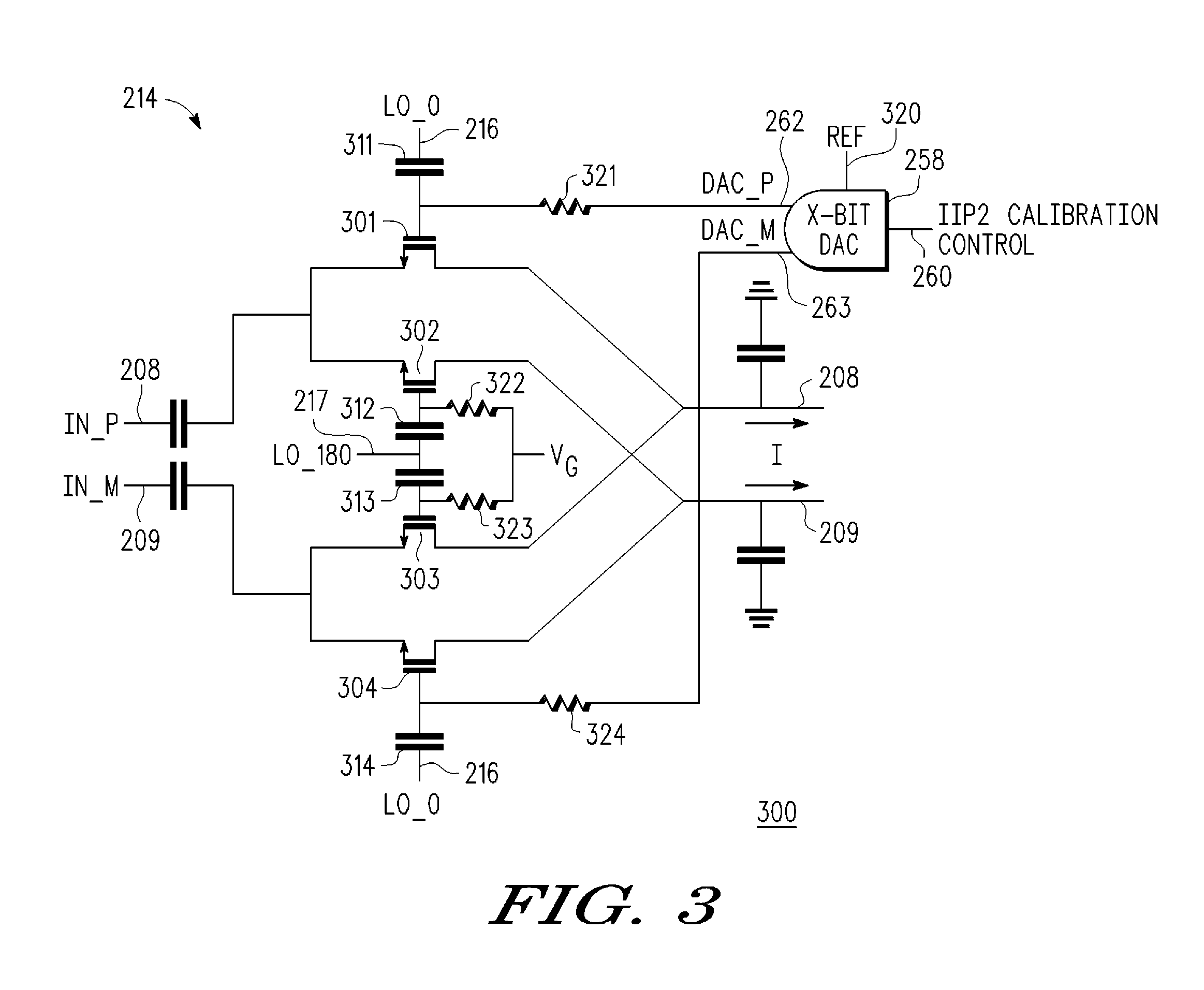
[0026]FIG. 3 is a schematic of a circuit 300 for the mixer 214. The circuit 300 illustrates a passive double balanced mixer comprising devices 301, 302, 303 and 304. The term “device” as used in this context means an active amplifying or switching device such as a transistor. In exemplary embodiments, the transistor is a CMOS transistor that includes gate, source and drain terminals. The term “passive” as used in this context, means that the mixer performs no amplification.

[0027]The circuit 300 includes an IN_P input node and an IN_M input node for receiving differential input signals IN_P 208 and IN_M 209, respectively, and two output nodes 220 and 221 for outputting differential output currents. The circuit also includes two balanced differential pairs. A first balanced differential pair includes first device 301 and second device 302 that have their sources coupled to the IN_P input node and their drains coupled to opposite output nodes. The drain of first device 301 is coupled t...

second embodiment

[0036]FIG. 4 is a schematic for a circuit 400 of the mixer 214. The circuit 400 illustrates a passive double balanced mixer comprising devices 301, 302, 303 and 304, wherein the IIP2 correction is introduced at the gate of device 301 and the gate of device 304, where the LO—0 signal and the LO—90 signal are injected. The circuit 400 includes a center tap 414 of resistors 415 and 416 across the output of the IP2 control DAC 258, which is used to provide the common-mode voltage that is applied to the gate of the devices 302 and 303 where the LO—180 signal is injected. Generating the gate bias voltage VG in this fashion tends to eliminate any common-mode offset caused by the IP2 control DAC 258. Advantageously, there is no temperature delta for the IP2 control DAC 258 because as R moves, I moves, and V stays the same.

[0037]In circuit 400, the bias voltage at the gates of devices 301 and 304 is the common-mode voltage plus the value of the IIP2 correction voltage, where the IIP2 correct...

third embodiment

[0038]FIG. 5 is a schematic for a circuit 500 of the mixer 214. The circuit 500 illustrates a passive double balanced mixer comprising devices 301, 302, 303 and 304, wherein the IIP2 correction is introduced at the gate of device 302 and at the gate of device 303, where the LO—180 signal is injected. In FIG. 5, the bias voltage at the gates of devices 302 and 303 are compensated to correct for IIP2 imbalance, as determined by the DSP 250. In FIG. 5, the bias voltage at the gates of devices 301 and 304 are uncompensated. The circuit 500 includes a center tap 414 of resistors 415 and 416 across the output of the IP2 control DAC 258, which is used to provide the bias voltage VG at the gate of the devices 301 and 304 where the LO—0 signal is injected. Alternatively, the circuit 500 does not include the center tap 414 of resistors 415 and 416 across the output of the IP2 control DAC 258, and, instead, uses the approach used in circuit 300 for providing the bias voltage VG at the gate of ...


PUM


Abstract

A balanced mixer circuit (300, 400, 500, 600, 700 and 800) in a baseband receiver (202) includes an oscillator circuit (212), a mixer (214 and 215), a digital-to-analog converter (258 and 259) and a digital signal processor (250). The mixer includes CMOS devices (301, 302, 303 and 304). In response to differential outputs from the mixer, the digital signal processor controls the digital-to-analog converter to output bias voltages for the gate of at least one of the CMOS devices of the mixer to compensate for imbalance in the differential output of the mixer that may be caused by mismatch among two or more CMOS devices of the mixer or caused by other reasons, in order to increase second order intercept point of the mixer.

Description

CROSS REFERENCE TO RELATED APPLICATIONS[0001]This is a divisional of application Ser. No. 12 / 028,720, filed Feb. 8, 2008. The entire disclosure of prior application Ser. No. 12 / 028,720 is hereby incorporated by reference.BACKGROUND OF THE INVENTION[0002]1. Field of the Invention[0003]This invention relates generally to radio frequency receivers, and more specifically to mixer circuits that reduce second order intermodulation distortion in a direct conversion receiver.[0004]2. Related Art[0005]A receiver uses the frequency response of a low noise amplifier (LNA), a surface acoustic wave (SAW) filter and a duplexer to attenuate signals that are far from a center frequency of the receiver sufficiently enough to not corrupt a desired signal. If the LNA and the SAW filter are removed from the analog line-up of the receiver, problems that can detrimentally affect the performance of the receiver may arise. In a transceiver, which comprises a transmitter and a receiver, one such problem is ...

Claims


Application Information

Patent Timeline
Patent Type & Authority Applications(United States)
IPC IPC(8): H04B1/26
CPCH03D7/165H04B1/30H04B1/109
Inventor KACZMAN, DANIEL L.SHAH, MANISH N.GOLAT, JOSEPH P.CONNELL, LAWRENCE E.
Owner NORTH STAR INNOVATIONS
Why Eureka
Try Eureka