Organic electroluminescene device

a technology of electroluminescence and organic el, which is applied in the direction of discharge tube luminescnet screen, organic semiconductor device, discharge tube/lamp details, etc., can solve the problems of difficult practical use of organic el, degraded light emission performance, low durability, etc., and achieve enhanced fluorescence and plasmon-enhanced organic electraluminescence

Active Publication Date: 2011-08-25
UDC IRELAND
View PDF4 Cites 12 Cited by
  • Summary
  • Abstract
  • Description
  • Claims
  • Application Information

AI Technical Summary

Benefits of technology

[0010]Further, A. Fujiki et al., “Enhanced fluorescence by surface plasmon coupling of Au nanoparticles in an organic electroluminescence diode”, Applied Physics Letters, Vol. 96, pp. 043307-1-043307-3, 2010 reports that, in an EL device, plasmon enhancement effect was obtained for a light emitting material having a very low quantum efficiency value of 5.0×10⁻⁸ to 2.0×10⁻⁸ by disposing Au fine particles with a particle diameter of 12 nm adjacent to a transparent electrode (ITO) used as the anode of the device.
[0011]But, in W. Li et al., “Emissive Efficiency Enhancement of Alqa and Prospects for Plasmon-enhanced Organic Electraluminescence”, Proc. of SPIE, vol. 7032, pp. 703224-1-703224-7, 2008, the emission enhancement due to the plasmon enhancement effect is confirmed only for photoexited light emitting devices (photoluminescence devices (PL devices)), and no report of successful example is found for field exited EL devices.
[0012]Further, A. Fujiki et al., “Enhanced fluorescence by surface plasmon coupling of Au nanoparticles in an organic electroluminescence diode”, Applied Physics Letters, Vol. 96, pp. 043307-1-043307-3, 2010 describes that higher plasmon enhancement effect was obtained for lower quantum efficiency. It is generally known that the plasmon enhancement effect can be obtained in a case w

Problems solved by technology

Light emitting materials used for organic EL, however, have a problem of low durability, which makes the organic EL difficult to be put into practical use.
It is known that organic materials inherently remain in exited state for a long time, whereby the chemical bonding of the materials is broken and the light emission performance is degraded with time.
This low durability is a big challenge in employing an organic substance to a light emitting device.
In this structure, the light incident on

Method used


Image

  • Organic electroluminescene device
  • Organic electroluminescene device
  • Organic electroluminescene device

Examples


first embodiment

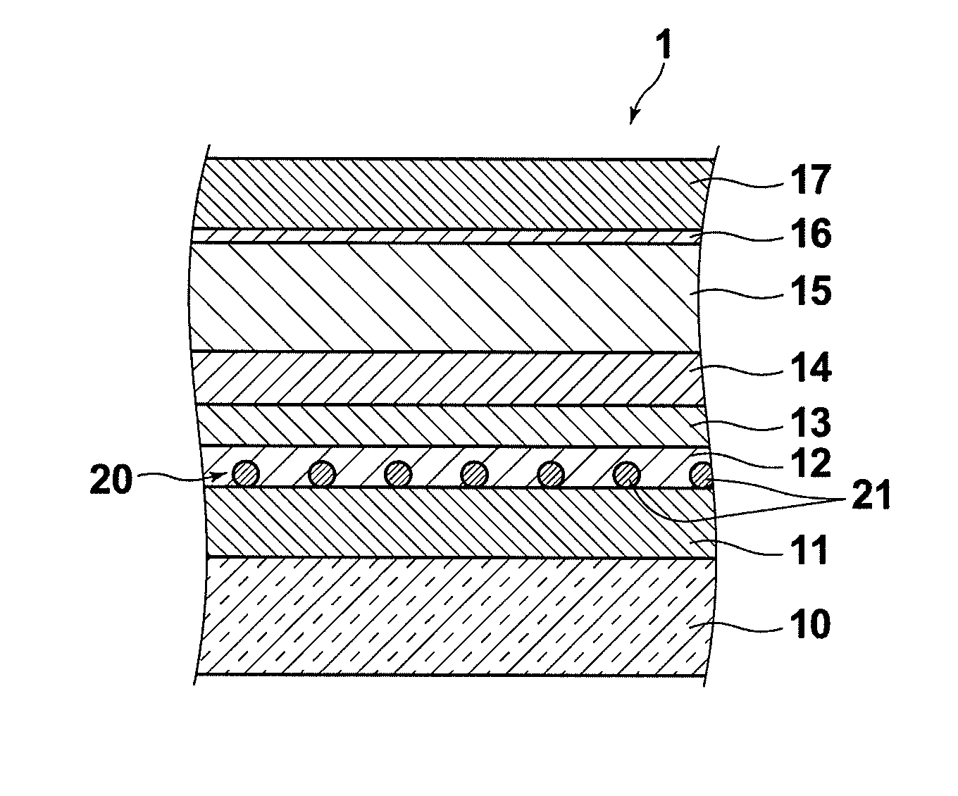
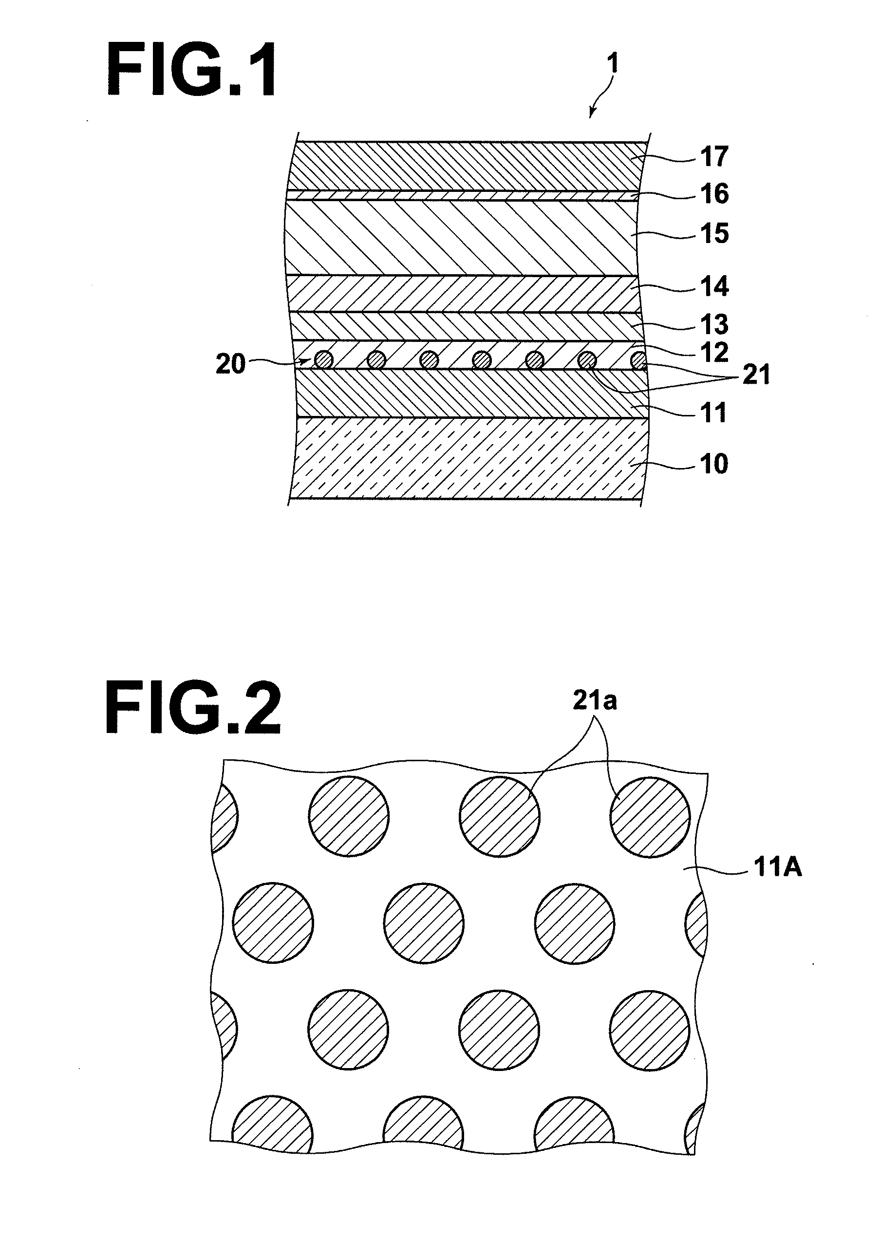
[0041]FIG. 1 is a cross-sectional view of organic EL device 1 according to a first embodiment of the present invention, schematically illustrating the structure thereof.

[0042]Organic EL device 1 of the present embodiment includes transparent substrate 10, formed of a glass or the like, on which anode 11 having an optical transparency, hole injection layer 12, hole transport layer 13, light emitting layer 14, electron transport layer 15, electron injection layer 16, and cathode 17 are laminated in this order. Device 1 further includes a metal structure 20 formed of metal fine particles 21 that generate plasmon resonance by the light emitted from light emitting layer 14. Metal fine particles 21 are disposed so as to contact the surface of anode 11 and hole injection layer 12, which is a conductive organic layer, is filled between metal fine particles 21. As for metal fine particles 21, particles having a scattering cross section σS with respect to emission light emitted from light emi...

second embodiment

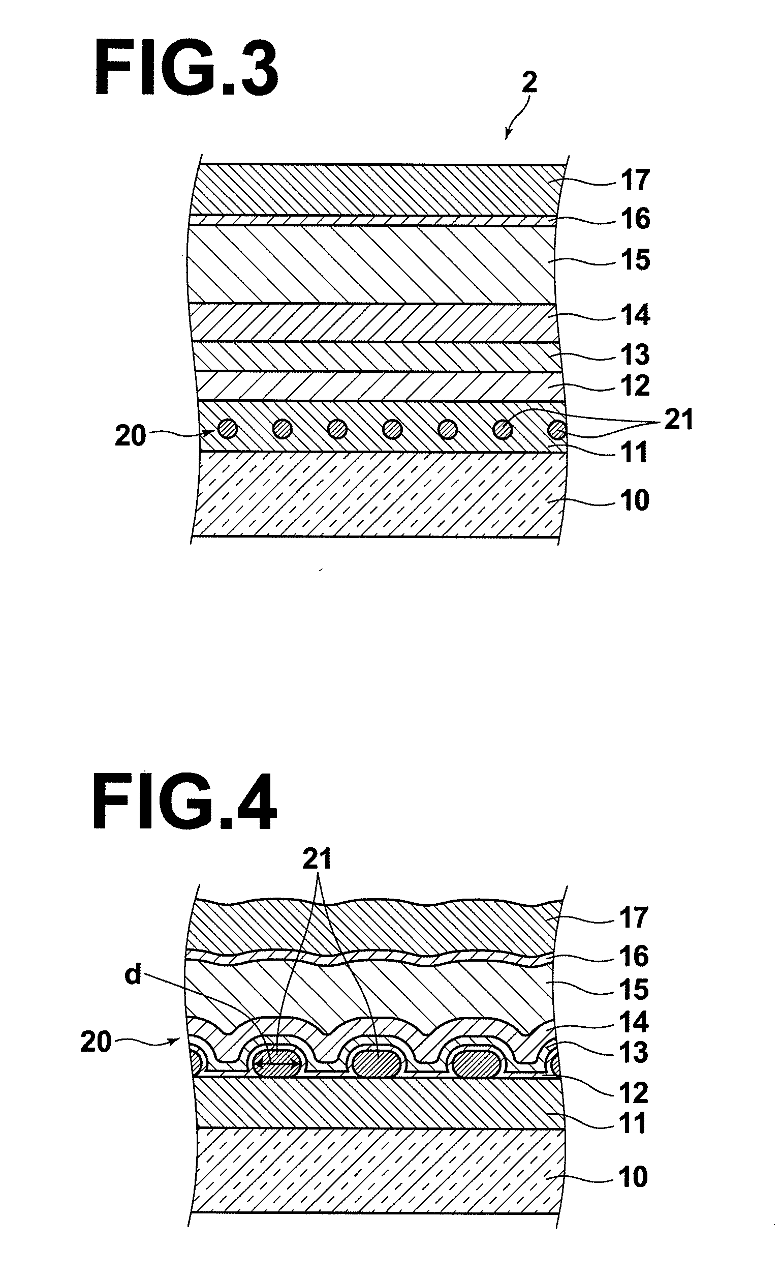
[0064]FIG. 3 is a cross-sectional view of organic EL device 2 according to a second embodiment of the present invention, schematically illustrating the structure thereof. Components identical to those of the organic EL device 1 in drawings that will be described hereinafter are given the same reference numerals.

[0065]Organic EL device 2 differs from organic EL device 1 according to the first embodiment in that metal structure 20 constituted by a plurality of metal fine particles 21 is disposed inside of anode 11 instead of on a surface of anode 11. In organic EL device 2, metal fine particles inside of anode 11 are disposed at a distance from light emitting layer 14 close enough to induce a plasmon resonance by the light emitted from light emitting layer 14.

[0066]In the present embodiment, anode 11 is formed of a transparent conductive material that does not generate a surface or local plasmon by the light emitted from light emitting layer 14 or a metal which is more unlikely to gen...

examples

[0072]Examples and Comparative Examples of the organic EL device of the present invention were produced and the following experiments were performed.


PUM


Abstract

An organic electroluminescence device having two electrodes and a plurality of organic layers between the two electrodes, in which the organic layers include a light emitting layer that emits light when an electric field is applied between the two electrodes. The device further includes a plurality of metal fine particles, which generates a local plasmon by light emitted from the light emitting layer, inside of at least either one of the electrodes or adjacent to a side of the electrode facing the organic layers and inside of a conductive organic layer, and at least some of the plurality of metal fine particles are disposed adjacent to the light emitting layer. Here, as the metal fine particles, particles having a scattering cross section σS which is larger than an absorption cross section σA thereof with respect to light emitted from the light emitting layer are used.

Description

CROSS-REFERENCE TO RELATED APPLICATION[0001]This application is a continuation-in-part application of U.S. patent application Ser. No. 12 / 700,167.BACKGROUND OF THE INVENTION[0002]1. Field of the Invention[0003]The present invention generally relates to a light emitting device (electroluminescence device) that emits light when an electric field is applied and more particularly to an organic electroluminescence device with improved light emitting efficiency.[0004]2. Description of the Related Art[0005]Recently, organic EL has been drawing attention for use in illumination, display light sources, and the like. Light emitting materials used for organic EL, however, have a problem of low durability, which makes the organic EL difficult to be put into practical use.[0006]It is known that organic materials inherently remain in exited state for a long time, whereby the chemical bonding of the materials is broken and the light emission performance is degraded with time. This low durability i...

Claims


Application Information

Patent Timeline
IPC IPC(8): H01J1/62
CPCH01L51/0072H01L51/0081H05B33/24H01L51/5262H01L2251/308H01L51/0085H10K85/6572H10K85/324H10K85/342H10K50/85H10K2102/103
Inventor YASUDA, HIDEKINAYA, MASAYUKI
Owner UDC IRELAND
Why Eureka
Try Eureka