Crosstalk mitigation in optical transceivers

a technology of optical transceivers and crosstalk mitigation, which is applied in electromagnetic transceivers, lasers, instruments, etc., can solve the problems of labor-intensive optical alignment and multiple packaging, the cost of optical alignment and volume scalability in the manufacturing of such components is increasing, and the deep penetration of optical fiber into access networks requires a massive deployment of optical interface equipmen

Inactive Publication Date: 2011-09-08
ONECHIP PHOTONICS
View PDF11 Cites 51 Cited by
  • Summary
  • Abstract
  • Description
  • Claims
  • Application Information

AI Technical Summary

Benefits of technology

[0019]The purpose of this invention is to provide a method of suppressing both optical and electrical crosstalk between the transmitter and receiver sections of either monolithically integrated optical transceiver PICs or hybrid i

Problems solved by technology

Deep penetration of optical fiber into access networks requires an unparalleled massive deployment of optical interface equipment that drives the traffic to and from users.
Therefore, cost efficiency and volume scalability in manufacturing of such components are increasingly major issues.
Within a framework of the current optical component manufacturing paradigm, which is based mainly on bulk optical sub-assemblies (OSA) from off-the-shelf discrete passive and active photonic devices, the root cause of the problem lies in a labor-intensive optical alignment and costly multiple packaging.
Not only do these limit the cost efficiency, but they also significantly restrict the manufacturer's ability to ramp production volumes and provide scalability in manufacturing.
However, in any implementation of an optical transceiver, performance degradation is evident in the receiver channel or channels as a result of crosstalk within the optical transceiver.
However, such elements increase the complexity of the optical implementations of the transceiver circu

Method used


Image

  • Crosstalk mitigation in optical transceivers
  • Crosstalk mitigation in optical transceivers
  • Crosstalk mitigation in optical transceivers

Examples


Embodiment Construction

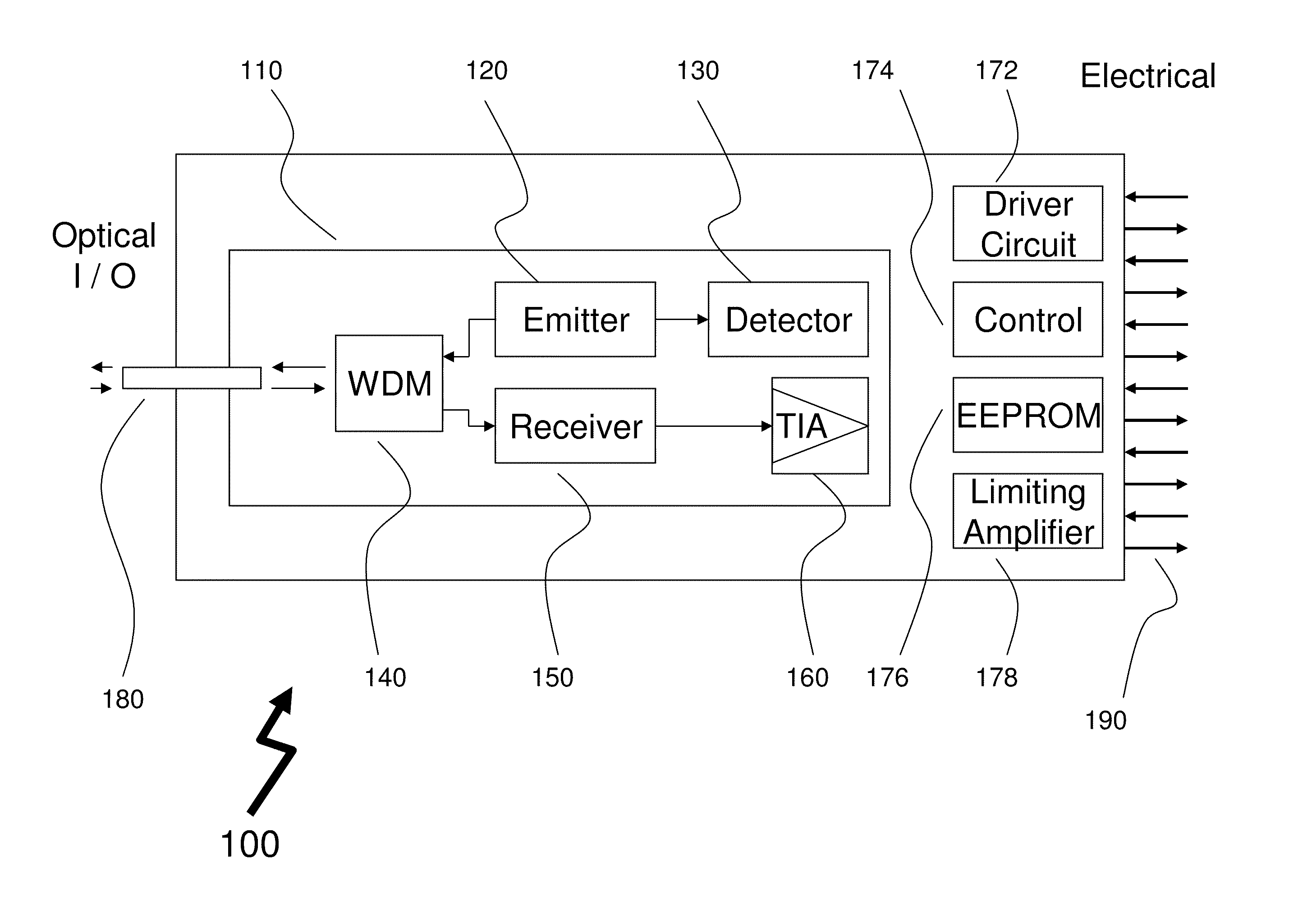
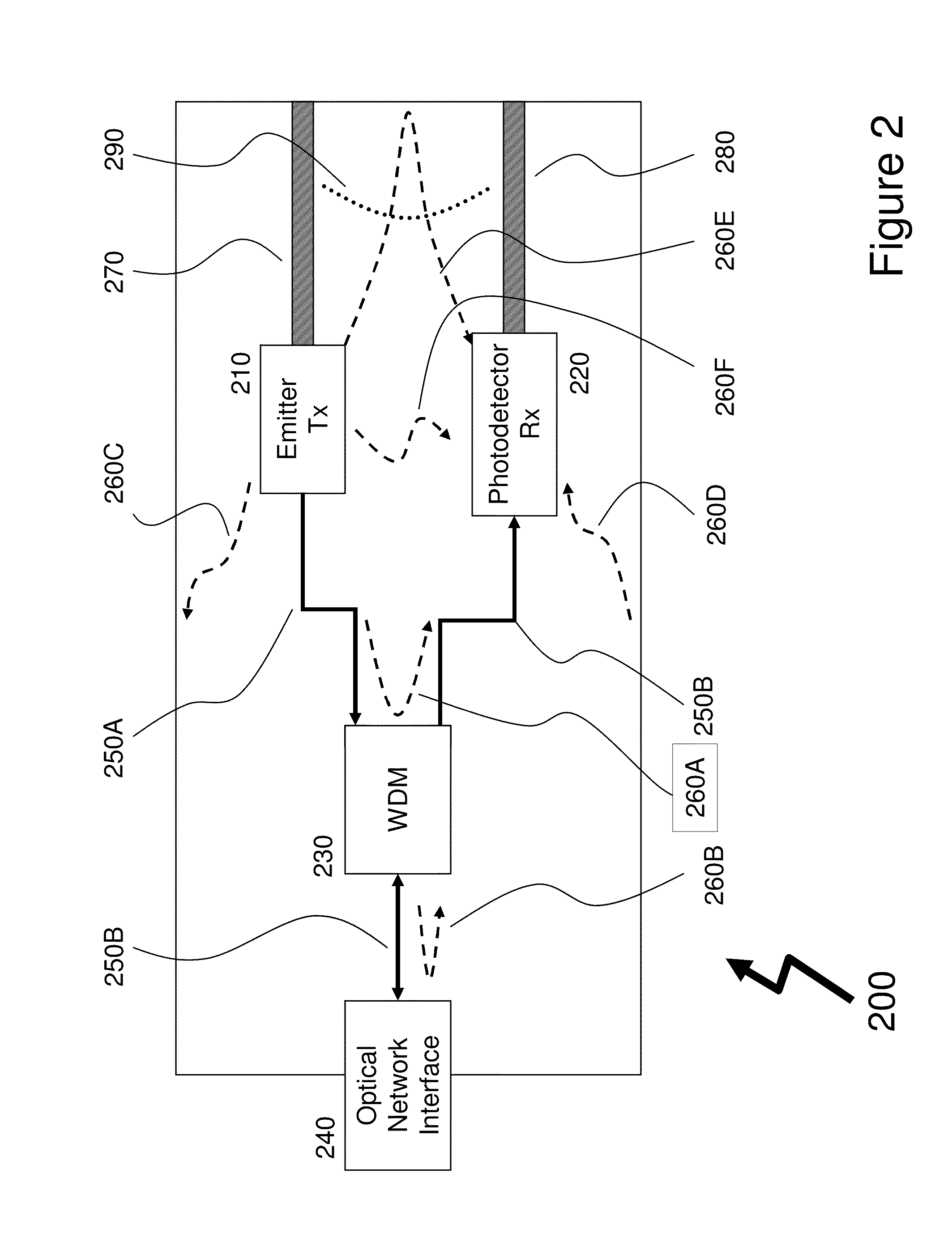
[0050]The present invention is directed to method of correcting a received signal from a primary photodetector with a correction signal derived from a secondary photodetector disposed in a predetermined relationship to the primary photodetector. The correction signal being substantially that of the primary photodetector minus the intended received signal for this primary photodetector, the secondary photodetector not receiving the intended received signal and thereby receiving only optical and / or electrical crosstalk. Accordingly combining the electrical signals from the primary and secondary photodetectors allows this crosstalk to be subtracted thereby improving the signal-to-noise ratio of the intended received signal.

[0051]Reference may be made below to specific elements, numbered in accordance with the attached figures. The discussion below should be taken to be exemplary in nature, and not as limiting of the scope of the present invention. The scope of the present invention is ...


PUM


Abstract

The invention relates to a method of improving the performance of optical receivers within optical transceivers by compensating for crosstalk, both optical and electrical. Optical crosstalk may arise within the optical receiver from a variety of sources including directly from the optical emitter within, indirectly from the optical emitter via losses, and losses of other received wavelengths within the optical transceiver coupled to the optical receiver. Electrical crosstalk may arise for example between the electrical transmission lines of the optical transmitter and optical receiver. The method comprises providing a secondary optical receiver in predetermined location to the primary optical receiver, the optical receivers being electrically coupled such that the crosstalk induced photocurrent in the secondary optical receiver is subtracted from the photocurrent within the primary optical receiver. The method may be applicable to either monolithic and hybrid optical transceivers.

Description

FIELD OF THE INVENTION[0001]This invention relates to optical transceivers and more specifically to mitigating optical and electrical crosstalk within such optical transceivers.BACKGROUND OF THE INVENTION[0002]Deep penetration of optical fiber into access networks requires an unparalleled massive deployment of optical interface equipment that drives the traffic to and from users. For example, optical transceivers, which receive downstream signals on one wavelength and send upstream signals on another wavelength, both wavelengths sharing the same optical fiber, have to be deployed at every optical line terminal (OLT), optical network unit (ONU), or optical network terminal (ONT). Therefore, cost efficiency and volume scalability in manufacturing of such components are increasingly major issues. It is broadly accepted within the telecommunication industry that optical access solutions are not going to become a commodity service, until volume manufacturing of the optical transceivers a...

Claims


Application Information

Patent Timeline
IPC IPC(8): H04J14/02
CPCG02B6/12002G02B6/12007G02B6/42H04B10/85H01S5/0264H04B10/40H01S5/026
Inventor WATSON, CHRISTOPHERVITIC, MICHAEL
Owner ONECHIP PHOTONICS
Why Eureka
Try Eureka