

Method for metalizing blind vias
a blind via and metalization technology, applied in the field of microelectronics, can solve the problems of metallization by serigraphy, inconvenient methods, and high cost of performing metallization
- Summary
- Abstract
- Description
- Claims
- Application Information
AI Technical Summary
Benefits of technology
Problems solved by technology
Method used
Image

Examples
first embodiment
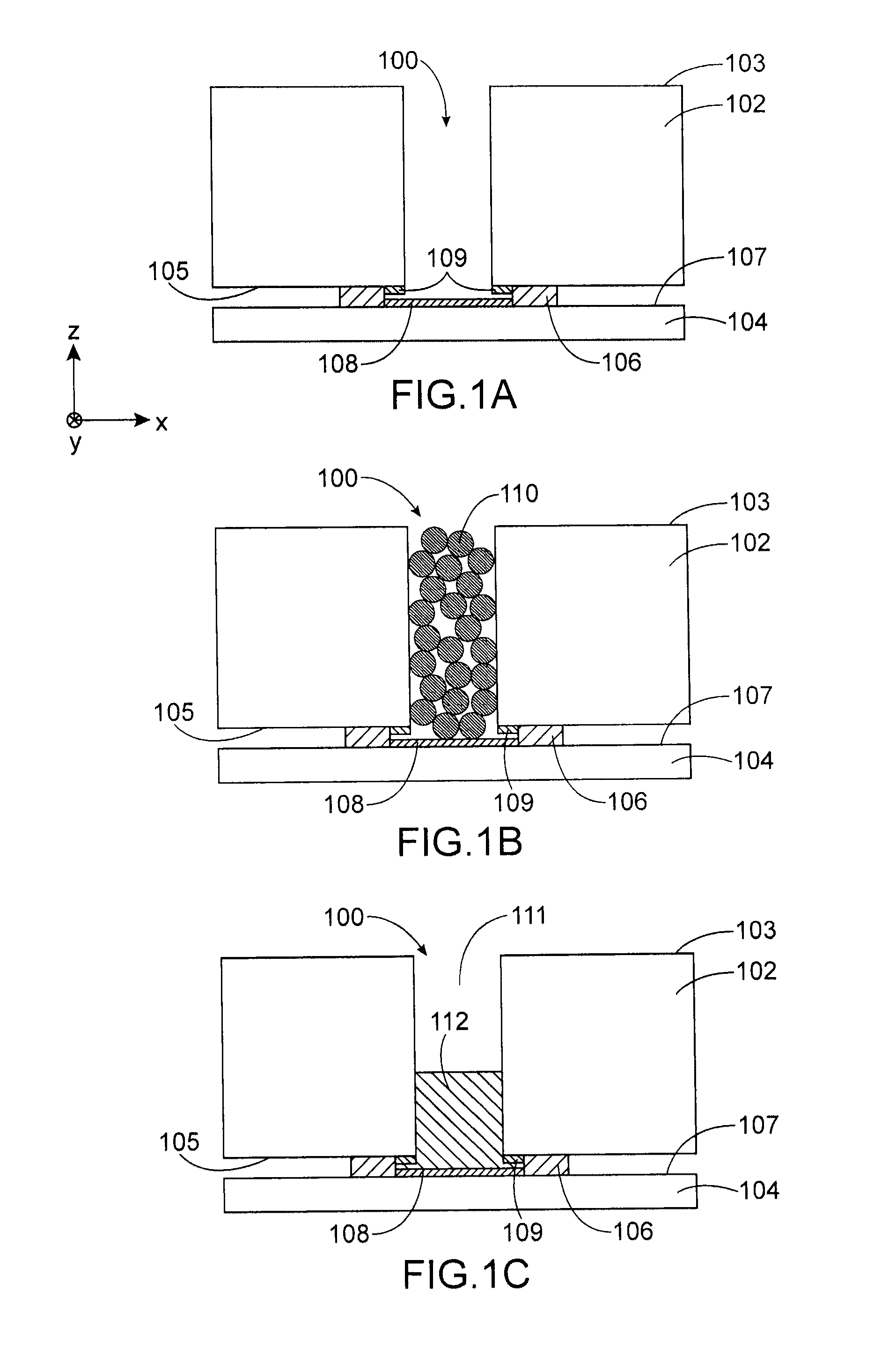
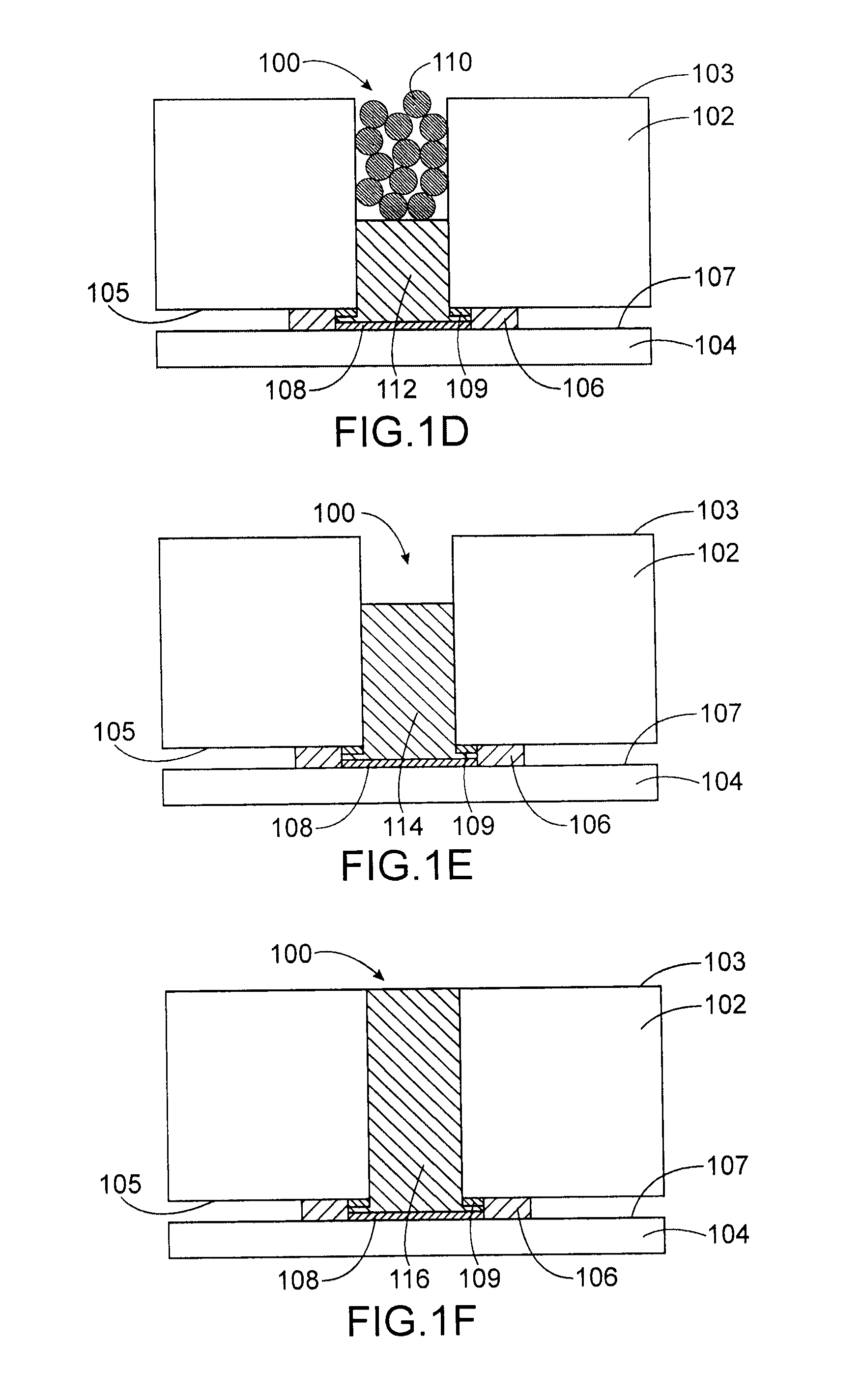
[0046]We will first refer to FIGS. 1A to 1F, which illustrate the steps of a method for metalizing a blind via 100 according to a
[0047]As shown in FIG. 1A, the blind via 100 is made in a structure including a first substrate 102 secured to a second substrate 104 by a sealing interface 106. The first and second substrates 102 and 104 are for example silicon-based and each have a thickness (dimension along the Z axis shown in FIG. 1A) equal to about 720 μm. The via 100 for example has a section, in the plane (X,Y) and at the level of the first substrate 102, substantially in the form of a disc and having a diameter for example equal to about 100 μm.
[0048]The via 100 passes through the first substrate 102 and therefore emerges both at an upper face 103 of the first substrate 102 and a lower face 105 of the first substrate 102. A bottom wall of the blind via 100 is formed by part of an upper face 107 of the second substrate 104 that is opposite the empty space formed by the via 100 in t...
second embodiment
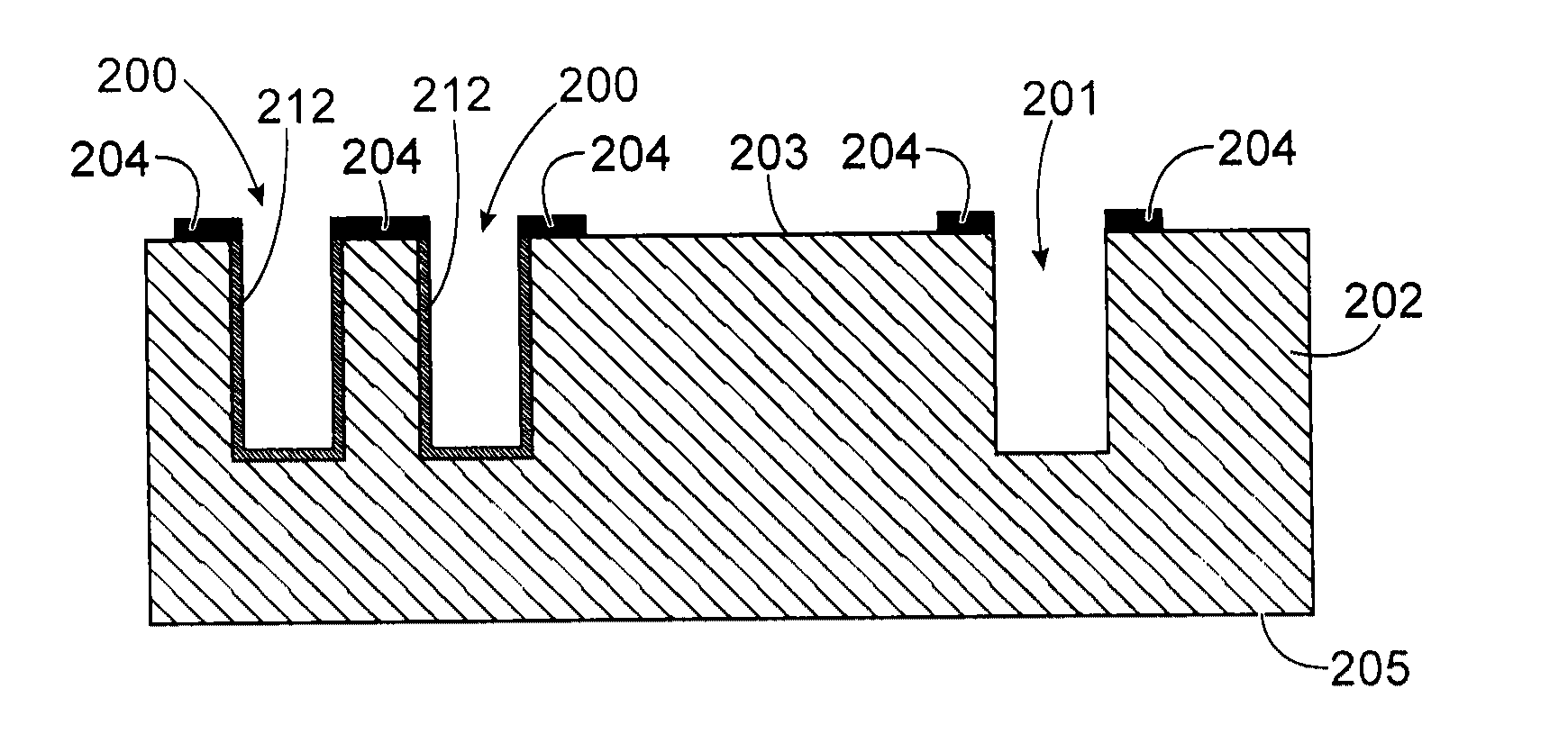
[0069]FIGS. 2A to 2D show the steps of a method for metalizing blind vias 200 according to a
[0070]As shown in FIG. 2A, the blind vias 200 are made in a substrate 202, for example of a nature and with dimensions similar to those of the first substrate 102 previously described. However, unlike the via 100, the vias 200 do not pass through the substrate 202 and each include a single opening at an upper face 203 of the substrate 202. Electrical contacts 204 are also made on the upper face 203 of the substrate 202, on the periphery of the openings of the vias 200. Another blind via 201, which we do not wish to metalize at the same time as the blind vias 200, is also made in the substrate 202.
[0071]Each of the blind vias 200 includes lateral walls 206 as well as a bottom wall 208 formed in the substrate 202. In this second embodiment, the lateral walls 206 and the bottom walls 208 of the vias 200 are treated so as to make them wetting relative to the electrically conductive material that ...
PUM
| Property | Measurement | Unit |
|---|---|---|
| diameters | aaaaa | aaaaa |
| diameter | aaaaa | aaaaa |
| thickness | aaaaa | aaaaa |
Abstract
Description
Claims
Application Information