

Plasma processing apparatus and plasma processing method
- Summary
- Abstract
- Description
- Claims
- Application Information
AI Technical Summary
Benefits of technology
Problems solved by technology
Method used
Image

Examples
embodiment 1
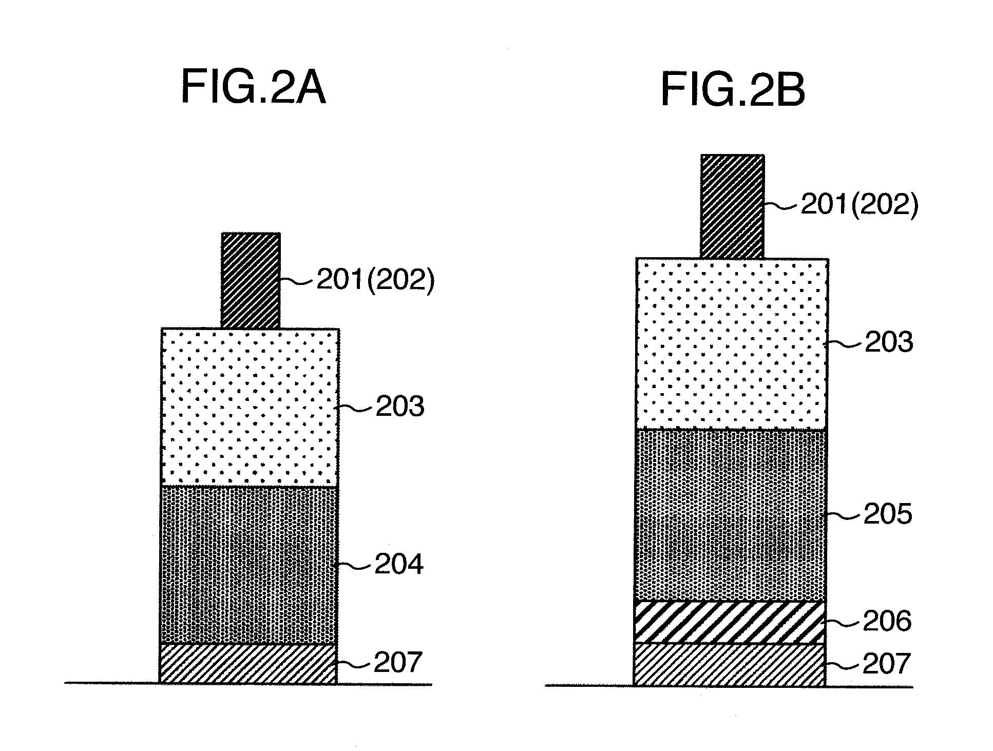
[0034]Embodiment 1 of the invention will now be described by making reference to FIGS. 1 to 10.
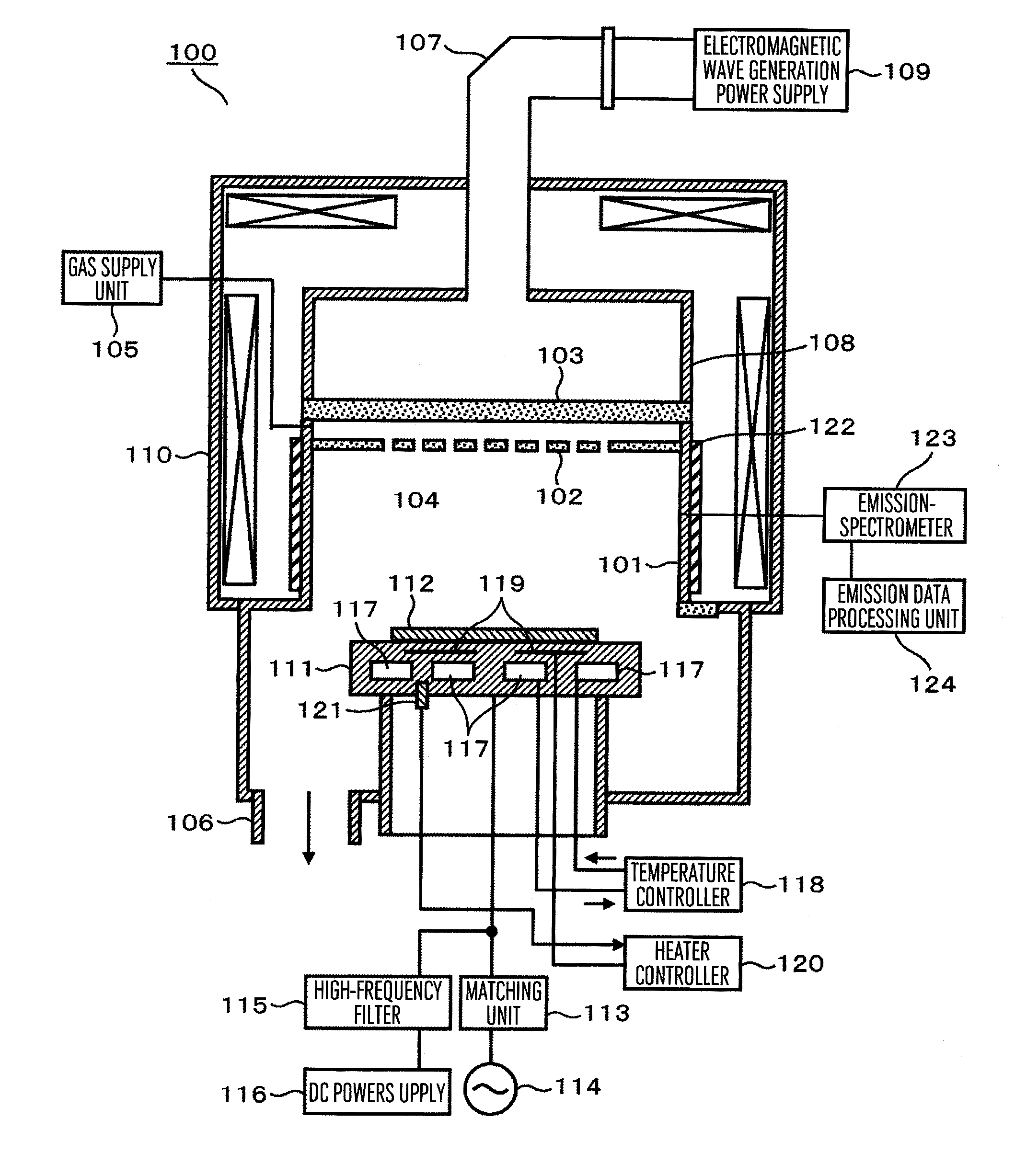
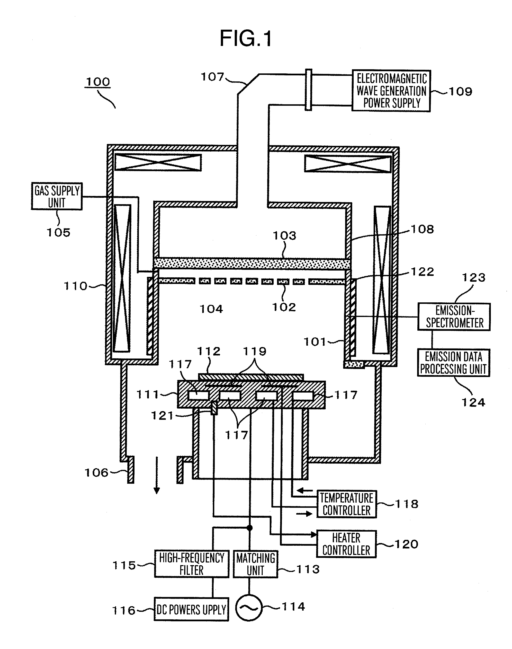
[0035]Reference will first be made to FIG. 1 showing a longitudinal sectional diagram for explaining the schematic construction of a plasma processing apparatus according to the present embodiment of the invention. Especially, in the present embodiment, an etching unit using microwave ECR (Electron Cyclotron Resonance) will be described.
[0036]In the plasma processing apparatus according to the present embodiment as shown in the figure, a shower plate 102 (for example, made of quartz or yttria) of circular disk form having a plurality of introduction holes arranged uniformly about a central portion and adapted to admit an etching gas to the interior of a vacuum chamber 101 and a dielectric window 103 (for example, made of quartz) are disposed at an upper portion of the vacuum chamber 101 opened upwards and the interior of a processing chamber 104 inside the vacuum chamber 101 and having a s...
PUM
 Abstract
Description
Claims
Application Information