Organic electroluminescent device

a technology of electroluminescent devices and organic el, which is applied in the direction of electroluminescent light sources, thermoelectric devices, electric lighting sources, etc., can solve the problems of reducing reducing the luminous efficiency of the device, and reducing the effect of reducing voltage, so as to reduce the power consumption of the organic el device, improve the luminous efficiency of the device, and reduce the driving voltage

Active Publication Date: 2011-09-29
SHARP KK
View PDF5 Cites 12 Cited by
  • Summary
  • Abstract
  • Description
  • Claims
  • Application Information

AI Technical Summary

Benefits of technology

[0015]According to the present invention, injection of holes into a light-emitting layer can be improved that matches the improvement of injection of electrons into the light-emitting layer, thereby making it possible to significantly lower driving voltage while maintaining or improving luminous efficiency of an organic EL device, while also enabling power consumption of the organic EL device to be reduced.

Problems solved by technology

The technology disclosed in Japanese Patent Application Laid-open No. 2005-26210 was unable to sufficiently prevent a decrease in luminous efficiency of the device while also impairing emission lifetime.
Although use of the technology disclosed in Japanese Patent Application Laid-open No. 2006-66872 certainly makes it possible to prevent deterioration of luminous efficiency or emission lifetime, as a result of limiting movement of electrons, the effect of reducing voltage is diminished, thereby preventing the inherent effect of reducing voltage from being adequately obtained.

Method used


Image

  • Organic electroluminescent device
  • Organic electroluminescent device
  • Organic electroluminescent device

Examples


example 1

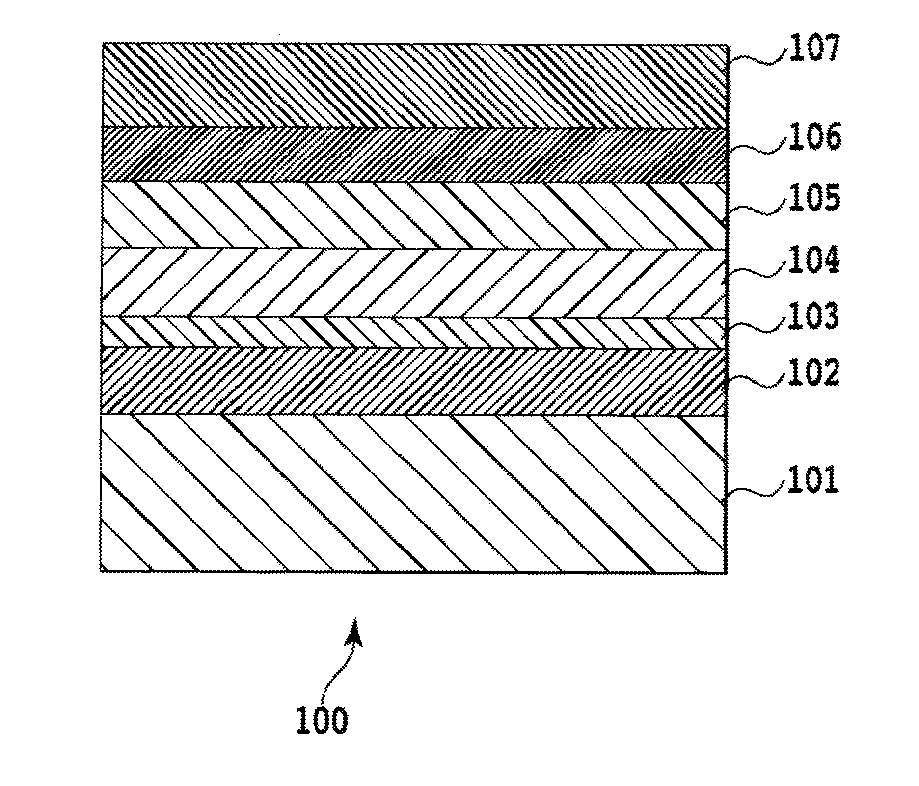
[0069]An IZO film was deposited on a glass substrate (50 mm long×50 mm wide×0.7 mm thick, Corning, 1737 glass) by DC Magnetron sputtering (target: In2O3+10 wt % ZnO, discharge gas: Ar+0.5% O2, discharge pressure: 0.3 Pa, discharge power: 1.45 W / cm2, substrate transport speed: 162 mm / min). This IZO film was then processed into the shape of stripes having a width of 2 mm by photolithography to form an IZO electrode having a film thickness of 110 nm and a width of 2 mm.

[0070]Next, a hole injection layer to which had been added an electron-accepting dopant was deposited on the IZO electrode. The deposition procedure consisted of simultaneously heating NPB and F4-TCNQ by resistance heating vapor deposition and simultaneously depositing using a vapor deposition rate for the F4-TCNQ of 0.02 Å / s versus a vapor deposition rate for the NPB of 1 Å / s to deposit a hole injection layer composed of an F4-TCNQ-doped NBP film at a thickness of 80 nm.

[0071]Continuing, TCTA was deposited to a thicknes...

example 2

[0075]A blue organic EL device was produced in the same manner as Example 1 with the exception of using a material in which p-TTA was doped with F4-TCNQ for the material of the hole injection layer. At this time, the vapor deposition rate of the p-TTA was 1 Å / s and the vapor deposition rate of the F4-TCNQ was 0.02 Å / s.

example 3

[0076]A blue organic EL device was produced in the same manner as Example 1 with the exception of using NPB for the material of the hole transport layer.


PUM


Abstract

An organic EL device is provided with a hole injection layer, a hole transport layer, a light-emitting layer, an electron transport layer and an electron injection layer between an anode and a cathode, wherein the hole injection layer is obtained by doping a hole transport material with an electron-accepting impurity, and the ionization potential Ip(HIL) of the material of the hole injection layer that composes the hole injection layer (also referred to as a hole injection material in the present description), the ionization potential Ip(HTL) of the hole transport material, and the ionization potential Ip(EML) of the material of the light-emitting layer (also referred to as a light-emitting layer material in the present description) respectively satisfy the relationship of Ip(EML)>Ip(HTL)≧Ip(HIL)≧Ip(EML)−0.4 eV.

Description

BACKGROUND[0001]The present invention relates to an organic electroluminescent device that can be applied to a flat panel display or illumination light source. More particularly, the present invention relates to an organic electroluminescent device that operates at a low driving voltage and has low power consumption.[0002]Research towards practical use of organic electroluminescent devices (hereinafter also referred to as organic EL devices) has been conducted actively in recent years. Since organic EL devices are able to realize high current density at low voltage, they are expected to be able to realize high emission luminance and luminous efficiency. These organic EL devices are provided with a first electrode and a second electrode surrounding an organic EL layer, and the electrode on the side on which light is extracted is required to have high transmittance. Normally transparent conductive oxide (TCO) materials (such as indium tin oxide (ITO), indium zinc oxide (IZO) or indium...

Claims


Application Information

Patent Timeline
Patent Type & Authority Applications(United States)
IPC IPC(8): H01L51/54
CPCH01L51/002H05B33/10H01L51/5088H01L51/5004H10K71/30H10K50/11H10K2101/40H10K50/17
Inventor TERAO, YUTAKAKANAI, NAOYUKI
Owner SHARP KK
Why Eureka
Try Eureka