Semiconductor apparatus, method of manufacturing semiconductor apparatus, method of designing semiconductor apparatus, and electronic apparatus

a semiconductor and design technology, applied in the direction of semiconductor devices, electrical devices, semiconductor/solid-state device details, etc., can solve the problems of impracticality, cost efficiency, complicated manufacturing process, etc., and achieve the effect of sufficiently exhibiting performance, inexpensively obtaining a semiconductor apparatus, and high performan

Active Publication Date: 2011-09-29
SONY CORP
View PDF16 Cites 143 Cited by
  • Summary
  • Abstract
  • Description
  • Claims
  • Application Information

AI Technical Summary

Benefits of technology

[0045]According to the present invention, a plurality of semiconductor wafers having circuits capable of achieving high performance and sufficiently exhibiting performance are stacked using an optimal process technique. Therefore, it is possible to inexpensively obtain a semiconductor apparatus hav

Problems solved by technology

However, since it is necessary to open the connection hole while insulation is secured in the deep or lower substrate, those techniques are impractical because they are not cost efficient in terms of the manufacturing process necessary for the processing of the connection hole and the bury the connection conductor.
In this case, the manufacturing process becomes complicated, and cost increases due to problems such as the necessity to attach an upper chip to the support substrate before the thinning.
Furthermore, in order

Method used


Image

  • Semiconductor apparatus, method of manufacturing semiconductor apparatus, method of designing semiconductor apparatus, and electronic apparatus
  • Semiconductor apparatus, method of manufacturing semiconductor apparatus, method of designing semiconductor apparatus, and electronic apparatus
  • Semiconductor apparatus, method of manufacturing semiconductor apparatus, method of designing semiconductor apparatus, and electronic apparatus

Examples


first embodiment

2. First Embodiment

[0108]Exemplary Configuration of Solid-State Imaging Apparatus and Exemplary Method of Manufacturing the Same

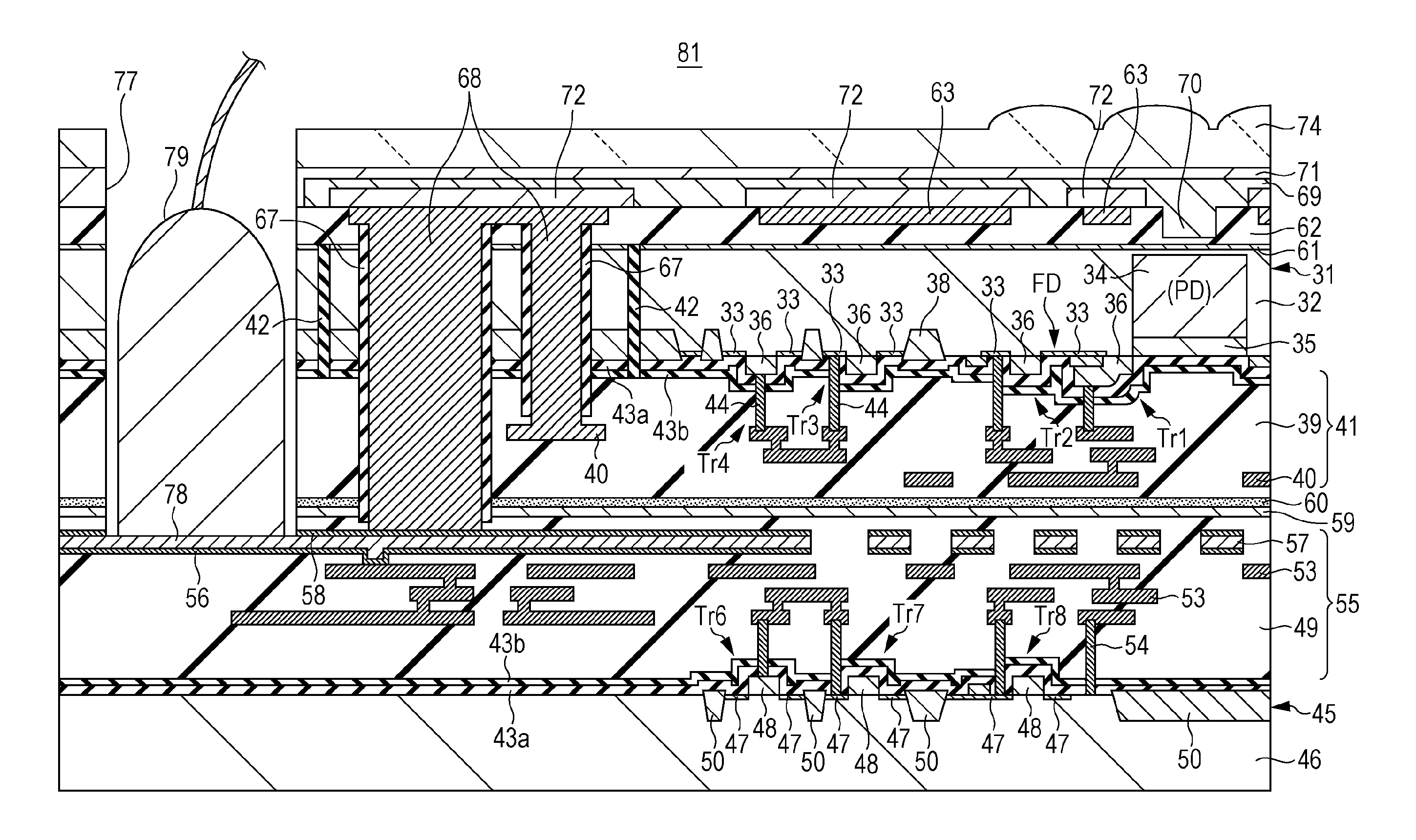
[0109]A rear-surface illuminated type MOS solid-state imaging apparatus as a semiconductor apparatus according to the first embodiment of the invention and a method of manufacturing the same will be described with reference to FIGS. 4 to 19.

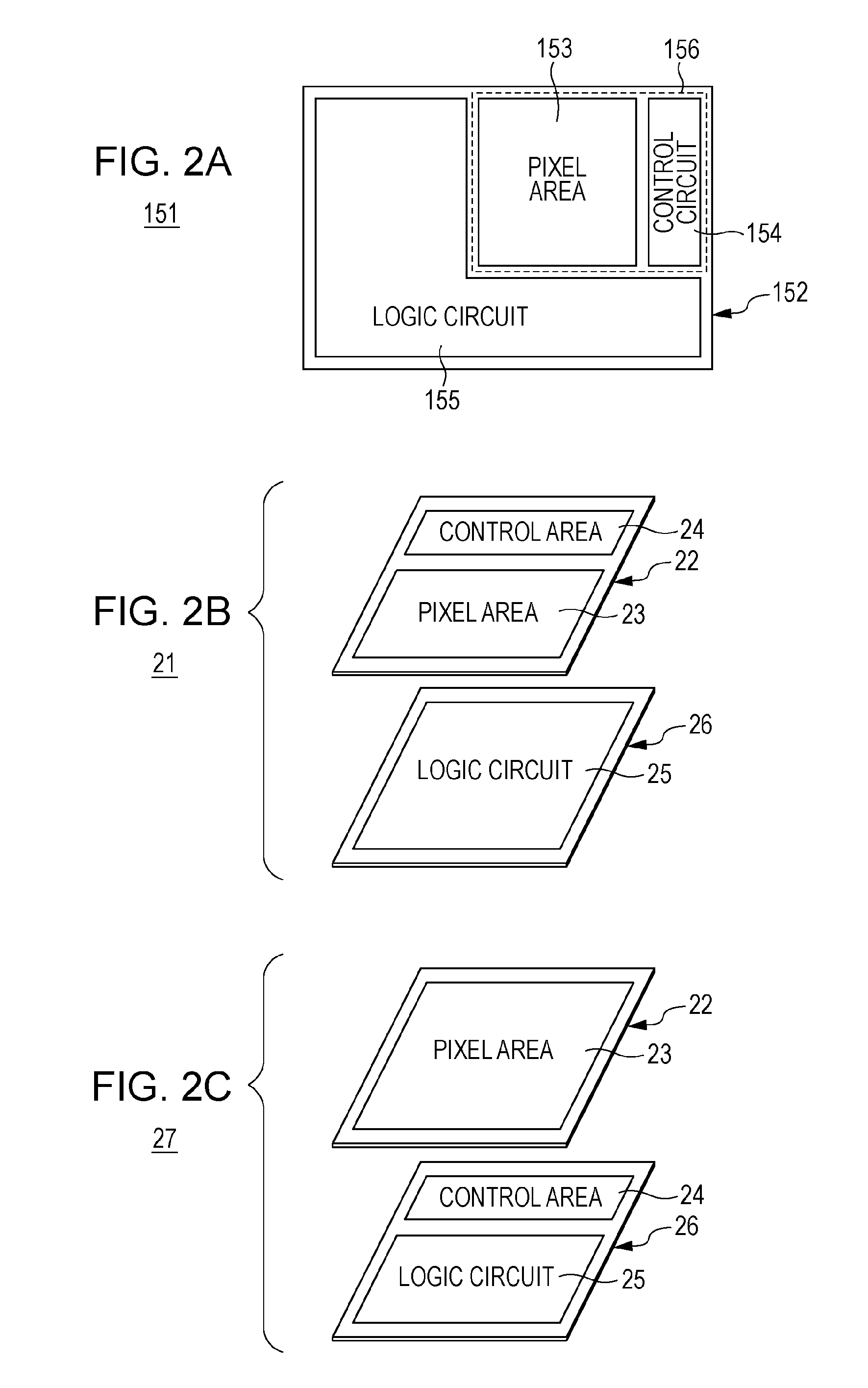
[0110]FIG. 4 is a schematic cross-sectional configuration diagram (completion diagram) including the electrode pad portion 78 of the solid-state imaging apparatus 81 according to an embodiment of the invention. The solid-state imaging apparatus 81 according to the an embodiment of the invention is obtained by vertically stacking a first semiconductor chip portion 22 where the pixel array (hereinafter, referred to as a pixel area) 23 and the control area 24 are included and a second semiconductor chip portion 26 where the logic circuit 25 is embedded while they are electrically connected to each other.

[0111]A method of ma...

second embodiment

3. Second Embodiment

Configuration Example of Semiconductor Apparatus and Method of Manufacturing the Same

[0174]A semiconductor apparatus and a method of manufacturing the same according to the second embodiment of the invention will be described with reference to FIGS. 20 to 26. The semiconductor apparatus 140 according to the present embodiment is obtained by stacking the first semiconductor substrate 101 having the first semiconductor integrated circuit and the second semiconductor substrate 102 having the second semiconductor integrated circuit. In FIG. 20, like reference numerals denote like elements as in FIG. 4, and descriptions thereof will not be repeated.

[0175]In the second embodiment, first, as shown in FIG. 21, a semi-finished first semiconductor integrated circuit, i.e., in this example, the logic circuit, is formed in the area corresponding to each chip portion of the first semiconductor substrate (semiconductor wafer) 101. Specifically, a plurality of MOS transistors T...

third embodiment

4. Third Embodiment

[0194]FIG. 27 is a schematic configuration diagram illustrating the solid-state imaging apparatus according to the third embodiment of the invention. In FIG. 27, like reference numerals denote like elements as in FIG. 4, and descriptions thereof will be omitted.

[0195]FIG. 27 illustrates an area including the pixel area 23 and the control area 24 of the solid-state imaging apparatus. For the purpose of simplification, some transistors and photodiodes are omitted.

[0196]As shown in FIG. 27, in the pixel area 23, the copper interconnect 40a which outputs a pixel signal formed in the first semiconductor substrate 31 is connected to the signal interconnect 57a formed in the interconnect of the uppermost layer of the second wiring layer 55 through the interconnect 68 between the first and second semiconductor substrates. In this case, in the circuit configuration shown in FIG. 3, the interconnect between the first and second semiconductor substrates is formed between the...


PUM


Abstract

A semiconductor device including a first material layer adjacent to a second material layer, a first via passing through the first material layer and extending into the second material layer, and a second via extending into the first material layer, where along a common cross section parallel to an interface between the two material layers, the first via has a cross section larger than that of the second via.

Description

CROSS-REFERENCE TO RELATED APPLICATIONS[0001]The present application claims priority to Japanese Priority Patent Application JP 2010-070925 filed in the Japan Patent Office on Mar. 25, 2010, the entire contents of which are hereby incorporated by reference.BACKGROUND OF THE INVENTION[0002]The present invention relates to a semiconductor apparatus such as a solid-state imaging apparatus, a method of manufacturing the same, a method of designing the same, and an electronic apparatus such as a camera having the solid-state imaging apparatus.[0003]An amplification type solid-state imaging apparatus representatively including a MOS type image sensor such as complementary metal oxide semiconductor (CMOS) is known in the art as a solid-state imaging apparatus. A charge transmission type solid-state imaging apparatus representatively including a charge coupled device (CCD) image sensor is also known in the art. Such solid-state imaging apparatuses are widely used in a digital still camera, ...

Claims


Application Information

Patent Timeline
IPC IPC(8): H01L31/0232H01L31/18H01L27/14
CPCH01L21/76898H01L2924/13091H01L27/14632H01L27/14634H01L27/14638H01L27/1469H01L21/76802H01L31/02002H01L24/05H01L2224/48463H01L2924/3025H01L23/481H01L2924/1306H01L2924/00H01L2224/02166H01L2224/04042H01L2924/12043H01L2924/14H01L2224/24147H01L2224/08145H01L2224/80896H01L2224/9202H01L2224/9212H01L27/14621H01L27/14627H01L27/14636H01L27/1464H01L27/14645H04N25/79H01L2224/03H01L2224/8203H01L2224/821H01L2224/80001H01L2224/82H01L23/535H01L23/5283H01L31/02013H01L31/02008
Inventor TAKAHASHI, HIROSHISUKEGAWA, SHUNICHIINOUE, KEISHI
Owner SONY CORP
Why Eureka
Try Eureka