Photoelectric conversion device and process for production thereof
- Summary
- Abstract
- Description
- Claims
- Application Information
AI Technical Summary
Benefits of technology
Problems solved by technology
Method used
Image

Examples
first embodiment
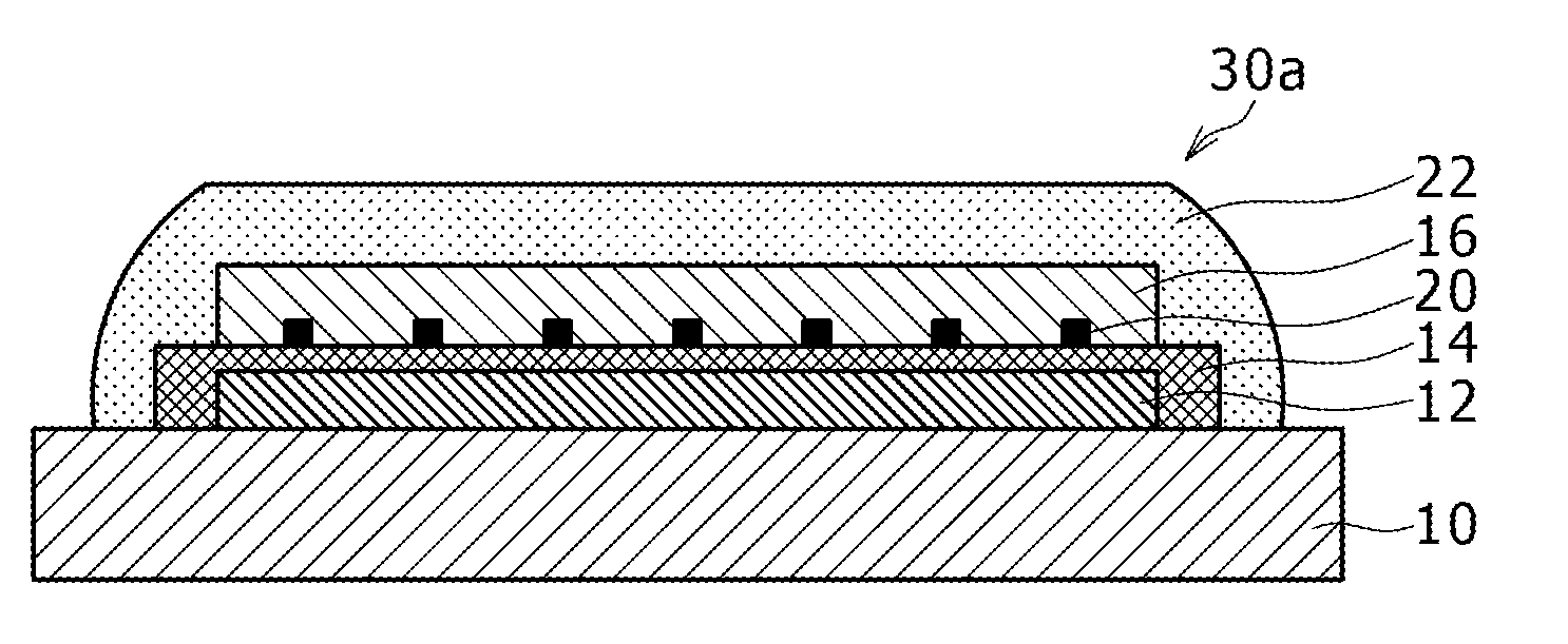
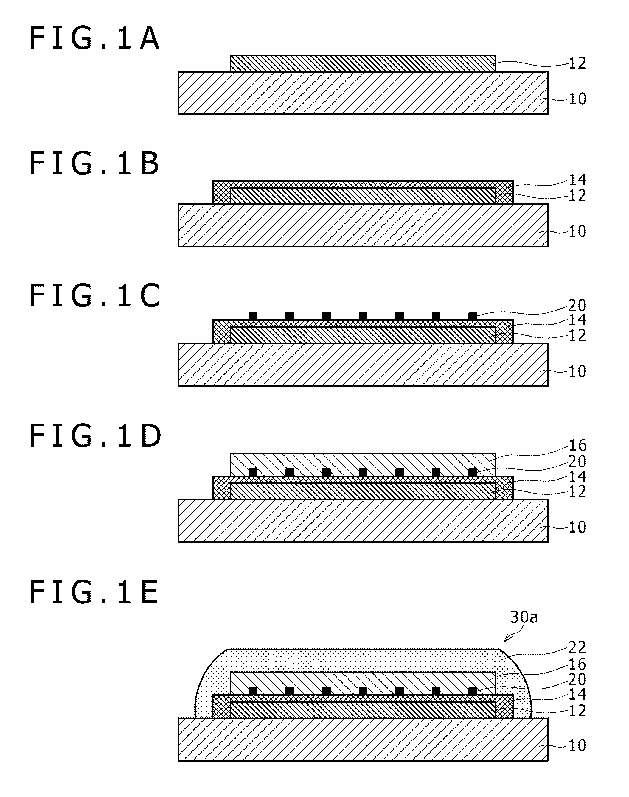
[0070]FIGS. 1A to 1E are diagrams illustrating the steps for production of the dye-sensitized solar cell element pertaining to the first embodiment of the present invention.
[0071]As shown in FIG. 1E, the dye-sensitized solar cell element 30a is composed of a substrate and functional layers sequentially formed thereon one over another. The substrate is the conductive sheet 10 of metal, such as Ti, in place of the glass substrate as the counter electrode. The functional layers include the porous carbon layer 12, the porous insulating layer 14, the current collecting grid 20, the porous metal oxide semiconductor layer 16, and the transparent sealing layer 22. The porous metal oxide semiconductor layer 16 contains a dye supported therein. The porous metal oxide semiconductor layer 16, the porous insulating layer 14, and the porous carbon layer 12 are impregnated with an electrolyte solution.
[0072]The porous carbon layer 12 is a catalyst layer. The porous insulating layer 14 is formed on...
second embodiment
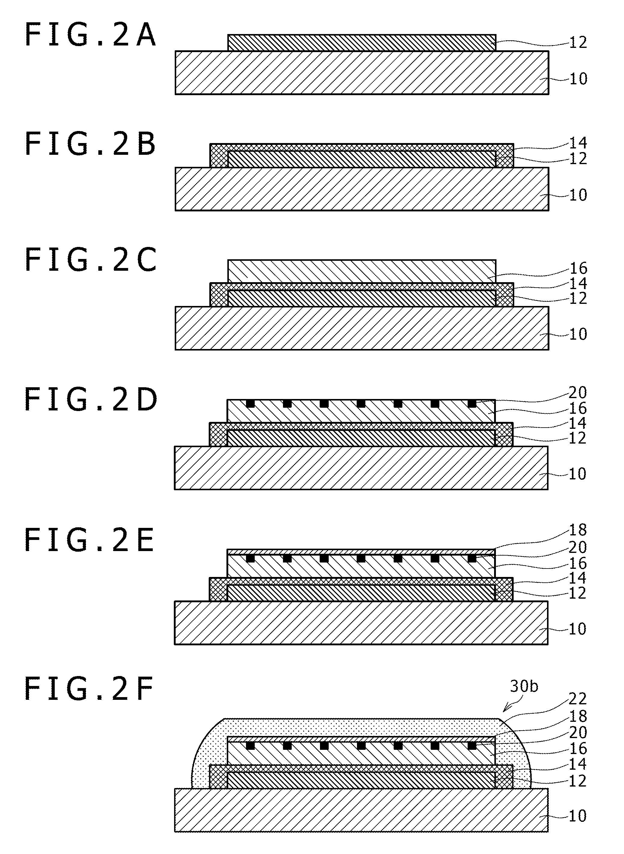
[0107]FIGS. 2A to 2F are diagrams illustrating the steps for production of the dye-sensitized solar cell element pertaining to the second embodiment of the present invention.
[0108]As shown in FIG. 2F, the dye-sensitized solar cell element 30b is composed of a substrate and functional layers sequentially formed thereon one over another, as in the case of the dye-sensitized solar cell element 30a shown in FIG. 1E. The substrate is the conductive sheet 10 of metal, such as Ti, in place of the glass substrate as the counter electrode. The functional layers include the porous carbon layer 12, the porous insulating layer 14, the porous metal oxide semiconductor layer 16, the current collecting grid 20, the transparent electrode layer 18, and the transparent sealing layer 22. The porous metal oxide semiconductor layer 16 contains a dye supported therein. The porous metal oxide semiconductor layer 16, the porous insulating layer 14 and the porous carbon layer 12 are impregnated with an elec...
third embodiment
[0134]FIGS. 3A to 3F are diagrams illustrating the steps for production of the dye-sensitized solar cell element pertaining to the third embodiment of the present invention.
[0135]As shown in FIG. 3F, the dye-sensitized solar cell element 30c is comprised of a substrate and functional layers sequentially formed thereon one over another, as in the case of the dye-sensitized solar cell elements 30a and 30b shown in FIGS. 1A to 1E and 2A to 2F, respectively. The substrate is the conductive sheet 10 of metal, such as Ti, in place of the glass substrate as the counter electrode. The functional layers include the porous carbon layer 12, the porous insulating layer 14, the porous metal oxide semiconductor layer 16, the transparent electrode layer 18, the current collecting grid 20, and the transparent sealing layer 22. The porous metal oxide semiconductor layer 16 contains a dye supported therein. The porous metal oxide semiconductor layer 16, the porous insulating layer 14, and the porous ...
PUM
 Abstract
Description
Claims
Application Information
 - Generate Ideas
- Intellectual Property
- Life Sciences
- Materials
- Tech Scout
- Unparalleled Data Quality
- Higher Quality Content
- 60% Fewer Hallucinations
Browse by: Latest US Patents, China's latest patents, Technical Efficacy Thesaurus, Application Domain, Technology Topic, Popular Technical Reports.
© 2025 PatSnap. All rights reserved.Legal|Privacy policy|Modern Slavery Act Transparency Statement|Sitemap|About US| Contact US: help@patsnap.com