Hybrid Group IV/III-V Semiconductor Structures

a semiconductor and hybrid technology, applied in the field of hybrid group iv/iii-v semiconductor structures, can solve the problems of severe material problems that have not been overcome, high cost of the ge-substrates on which they are fabricated, and excess photogenerated current in the ge subcell, etc., to achieve the effect of reducing cost, improving efficiency, and reducing the cost of the si substra

Inactive Publication Date: 2011-10-20
ARIZONA STATE UNIVERSITY
View PDF14 Cites 419 Cited by
  • Summary
  • Abstract
  • Description
  • Claims
  • Application Information

AI Technical Summary

Benefits of technology

[0008]The present disclosure is based on growth of device-quality Ge, Ge1-xSnx, and Ge1-x-ySixSny alloys on Si substrates. The photovoltaic potential of these materials arises from the low cost of the Si substrates and from the ability of Sn-containing materials to absorb solar infrared radiation and act as templates for subsequent growth over a wide range of lattice constants. Specifically, herein we have developed materials that bring about dramatic reductions in cost and increased efficiencies in hybrid group IV / III-V solar cells and in crystalline Si solar cells.

Problems solved by technology

Such a breakthrough would open up an enormous market for this technology, which so far has been limited to niche applications such as power production in space.
These systems suffer from two basic limitations: the high cost of the Ge-substrates on which they are fabricated and excess photogenerated current in the Ge subcell.
The Ge-current can be reduced by lowering the band gap of the middle cell, but this requires a higher In concentration that introduces a severe lattice mismatch.
So far the main candidate for this additional junction has been InGaAsN, but this system has severe materials problems that have not been overcome to date.
However, in all of these cases, however, the Ge materials were not active components of the multijunction cell.
An additional problem in these structures is the generation of wafer bowing due to the large thermal expansion mismatch between Ge and Si.
Unfortunately, up to now there were no suitable materials available possessing this property, with the possible exception of GaAsN alloys, which due to a “giant bowing” effect can have a band gap below that of GaAs (see, Wei and Zunger, Phys. Rev. Lett. 1996, 76, 664).
However, attempts to incorporate these alloys as a fourth junction have not been very successful due to material quality problems

Method used


Image

  • Hybrid Group IV/III-V Semiconductor Structures
  • Hybrid Group IV/III-V Semiconductor Structures
  • Hybrid Group IV/III-V Semiconductor Structures

Examples


example 1

Ge / Si(100) Structures and Templates

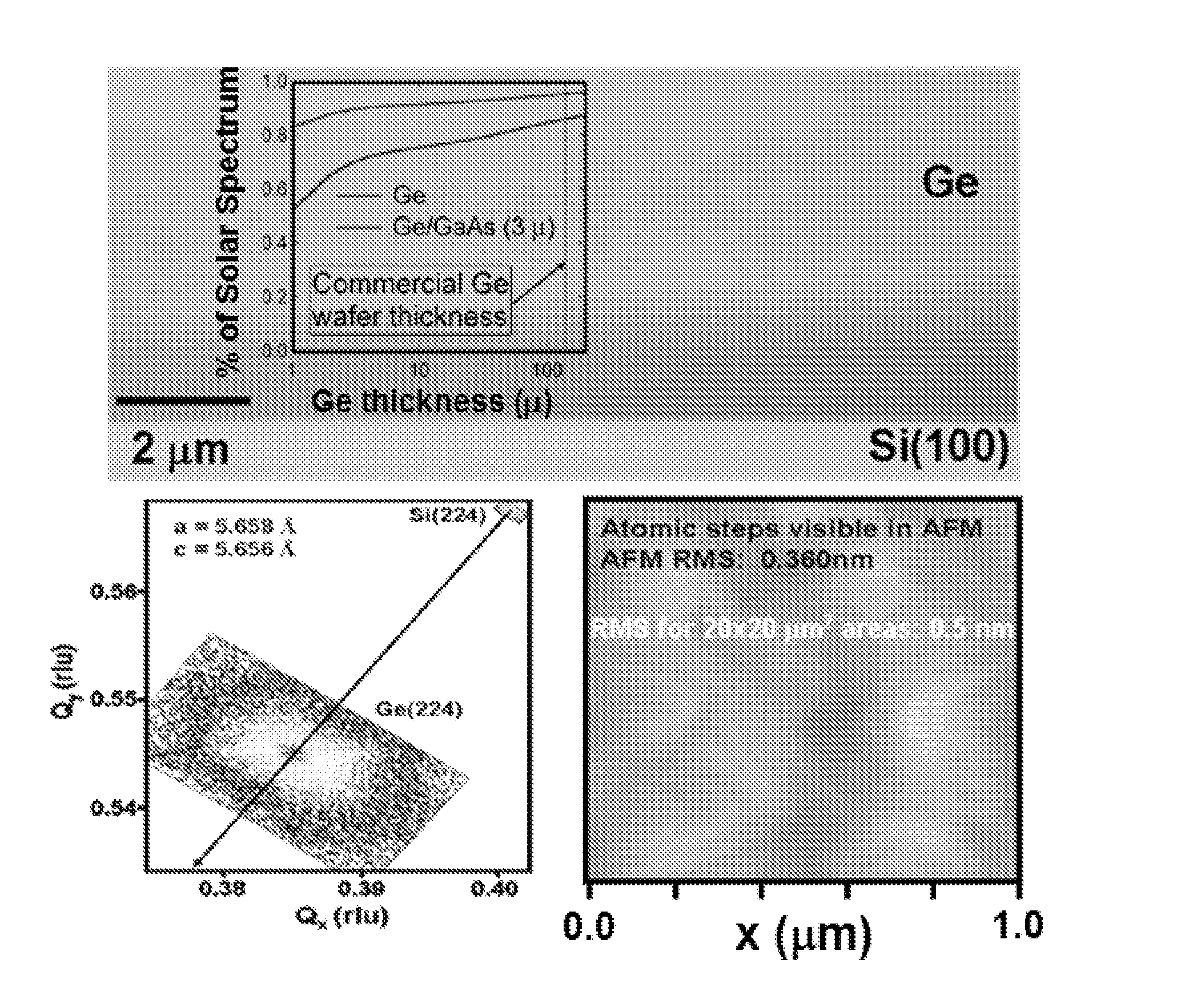
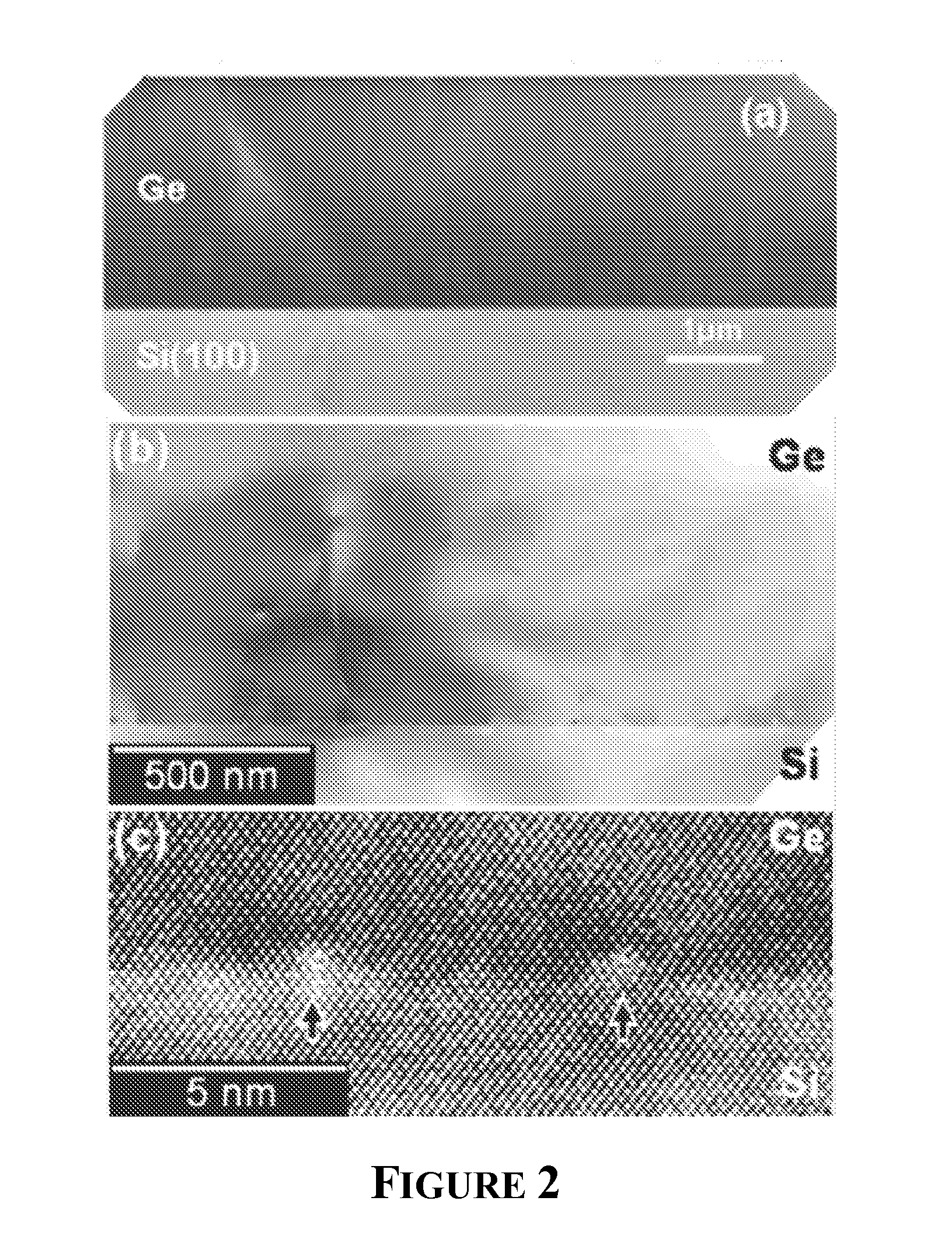
[0110]Pure Ge films can be formed directly on Si substrates with unprecedented control of film microstructure, morphology, purity and optical properties can be grown via CVD (see, Wistey et al., Appl. Phys. Lett. 2007, 90, 082108; and Fang et al., Chem. Mater. 2007, 19, 5910-25, which is hereby incorporated by reference in its entirety). In preceding method, growth is conducted at low temperatures (about 350° C. to about 420° C.) on a single wafer reactor configuration at 10−5-10−4 Torr, in the absence of gas phase reactions using molecular mixtures of Ge2H6 and small amounts of highly reactive (GeH3)2CH2 or GeH3CH3 organometallic additives.

[0111]The optimized molar ratios of these compounds have enabled layer-by-layer growth at conditions compatible with selective growth, which has recently been demonstrated by depositing patterned Ge “source / drain” structures in prototype devices. The driving force for this reaction mechanism is the facile elimin...

example 2

Doped Ge / Si(100)

[0116]The n-type doping of the Ge layers grown directly on Si can be conducted using proven protocols that have already led to the successful doping of the Ge1-xSnx alloys. These utilize As, Sb, P custom prepared hydride compounds such as As(GeH3)3, P(GeH3)3 and Sb(GeH3)3 molecules. These are co-deposited with mixtures of digermane to form Ge films incorporating the appropriate carrier type and level. In the case of As we have able to introduce free carrier concentrations as high as 1020 / cm3 in Ge1-xSnx via deposition of As(GeH3)3. These carbon-free hydrides are ideal for low temperature, high efficiency doping applications. They are designed to furnish a structural Ge3As unit resulting inhomogeneous substitution at high concentrations without clustering or segregation. For p-type doping suitable concentrations of gaseous B2H6 can be mixed with the Ge precursors and reacted to obtain the desired doping level.

[0117]In one example, p-type Ge layers with thickness of ab...

example 3

Optoelectronic Ge1-ySny Alloys

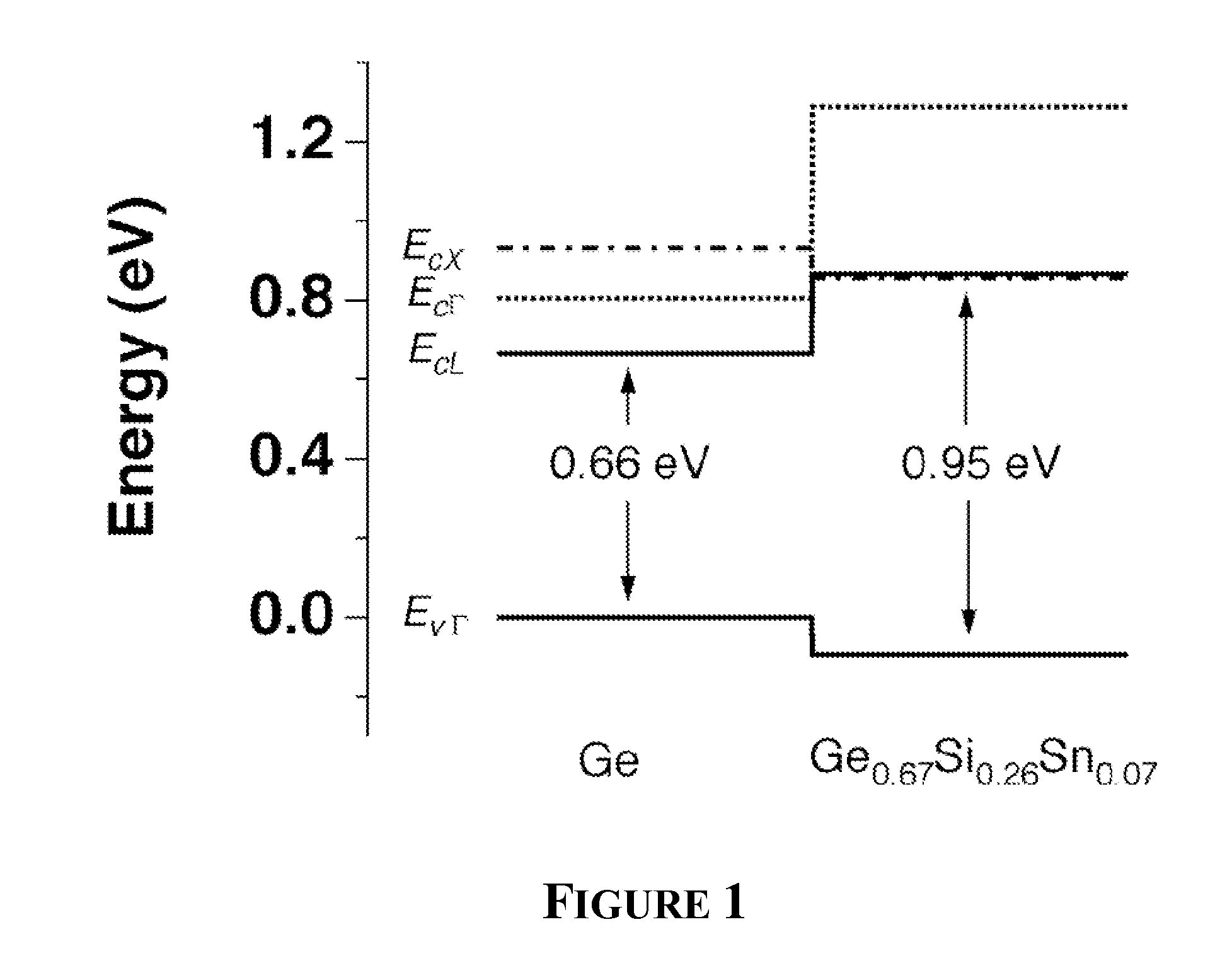
[0120]From a fundamental view point Ge1-ySny alloys on their own right are intriguing IR materials that undergo an indirect-to-direct band gap transition with variation of their strain state and / or compositions. They also serve as versatile, compliant buffers for the growth of II-VI and III-V compounds on Si substrates.

[0121]The fabrication of the Ge1-ySny materials directly on Si wafers has recently been reported using a specially developed CVD method involving reactions of Ge2H6 with SnD4 in high purity H2 (about 10%). Thick and atomically flat films are grown at 250° C. to about 350° C. and possess low densities of threading dislocations (about 105 cm−2) and high concentrations of Sn atoms up to about 20%. Since the incorporation of Sn lowers the absorption edges of Ge, the Ge1-ySny alloys are attractive for detector and photovoltaic applications that require band gaps lower than that of Ge (0.80 eV). The absorption coefficient of selected Ge1-xSnx s...


PUM


Abstract

Described herein are semiconductor structures comprising (i) a Si substrate; (ii) a buffer region formed directly over the Si substrate, wherein the buffer region comprises (a) a Ge layer having a threading dislocation density below about 105 cm−2; or (b) a Ge1-xSnx layer formed directly over the Si substrate and a Ge1-x-ySixSny layer formed over the Ge1-xSnx layer; and (iii) a plurality of III-V active blocks formed over the buffer region, wherein the first III-V active block formed over the buffer region is lattice matched or pseudomorphically strained to the buffer region. Further, methods for forming the semiconductor structures are provided and novel Ge1-x-ySixSny, alloys are provided that are lattice matched or pseudomorphically strained to Ge and have tunable band gaps ranging from about 0.80 eV to about 1.4O eV.

Description

CROSS-REFERENCE TO RELATED APPLICATIONS[0001]This application claims the benefit of the filing date of U.S. Provisional Application Ser. No. 61 / 105,670, filed Oct. 15, 2008, which is hereby incorporated by reference in its entirety.STATEMENT OF GOVERNMENT FUNDING[0002]The invention described herein was made in part with government support under grant number FA9550-60-01-0442, awarded by the US-AFOSR and the Department of Energy under Grant No. DE-FG36-08GO1800. The United States Government has certain rights in the invention.FIELD OF THE INVENTION[0003]The invention generally relates to semiconductor structures comprising Group IV and III-V semiconductor layers. In particular, the invention relates to the use of such structures as active components in solar cell designs.BACKGROUND OF THE INVENTION[0004]Monolithic multijunction solar cells have recently achieved efficiencies as high as 40.7%. (see, Martin and Green, Progress in Photovoltaics: Research and Applications 2006, 14, 455) ...

Claims


Application Information

Patent Timeline
Patent Type & Authority Applications(United States)
IPC IPC(8): H01L29/12H01L21/20
CPCH01L21/02381Y02E10/547H01L21/02452H01L21/02543H01L21/02546H01L21/02549H01L21/0262H01L31/0324H01L31/0687H01L31/076H01L31/105H01L31/1804H01L31/1844H01L31/1852Y02E10/544Y02E10/548H01L21/0245Y02P70/50
Inventor KOUVETAKIS, JOHNMENENDEZ, JOSE
Owner ARIZONA STATE UNIVERSITY
Why Eureka
Try Eureka